
 Eric Virey is from Yole Développment, a market research consultancy. and he spoke about Microled. (We have reported data from Yole in Display Daily – MicroLED Heads for Commercialisation)
Sony showed a FullHD 55″ TV at CES using microLEDs a few years ago and has used some of what it learned in its Cledis display (although Yole defines this as chip on board, rather than MicroLED).
There is a lot of activity going on with Apple, Oculus and Foxconn all investing in companies and there are a lot of patents already in the field.
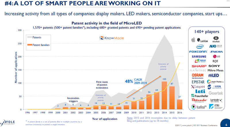 Yole said there is a lot of patent activity in MicroLED
You can make between five and twelve 4K displays from a single 6″ wafer and the process is generally to make the LEDs on the wafer, then spread them out on a TFT backplane. Materials are more efficient and more rugged than OLEDs. You get the great black of OLED, but you can also get up to 100K cd/m² of brightness and better colour than OLED (but not as good as QDs). High refresh rates and wide viewing angles are normal for microLED and it’s possible to integrate a wide range of sensors along with the pixels.
MicroLEDs can be made in a wide range of pixel spacing from 100 micron (for TV) down to 5 micron. For microdisplays, you can just use the wafer, with the LEDs as created, but if you want to make a TV, you have to distribute the LEDs across the backplane. There are dozens of patents around the different ways of doing this from elecrostatic processing, elastomer stamps and magnetic or fluidic self-assembly.
Typical LED making is very efficient, but the “harsh” processes used to make them cause defects that are not significant on a ‘big’ traditional LED, but a 1 micron defect could be a problem on a 5 x 5 micron chip, Virey said.
There have been some interesting claims about commercialisation in the last six months. However, there are a lot of issues in making these displays and the more you dig, the more you find.
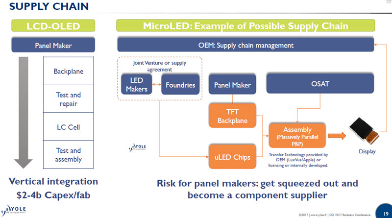
Virey started researching with the supply chain. There is a big LED industry already. However, microLEDs can’t be made in traditional fabs because of the need for much better clean rooms (because of the defect issue mentioned above). You also need better lithography. At the moment, it’s not obvious who will invest in the fabs needed (except in China).
Semiconductor foundries, on the other hand, might be able to make LEDs in older chip fabs, which have the right level of clean room.
For the backplane, a standard OLED LTPS or oxide backplane might be used. Some changes might be needed, but they are small.
The assembly plants need to be developed and new inspection and testing is needed. It’s not clear that any single company could take on the full microLED process. MicroLED may have a more horizontal supply chain and panel makers could get squeezed out to being just a backplane supplier. Others may capture most of the value.
Finally in applications the cost drivers are different. The cost scales with number of pixels not area (although backplane scales with area) (we have talked about this – What LED Has to Do to Be Truly Disruptive). Smartwatches and wearables may be the first application – there not too many pixels needed and the displays can be small in area.
Apple could probably get started with capex of $200 million to create a supply chain for its smartwatches. AR/MR applications could be good a good application because of the high brightness needed. Initially, AR & MR will be an enterprise market, so pricing is not too fierce, although it would need to be cheap for consumers. MicroLED might be the only technology that can meet the market need.
2019 could see some wearables or AR applications and Virey said in questions that it could take 18 months or two years for companies to compete with Sony’s Cledis LED technology.
Smartphones will be the hardest market to enter and there is still chance of a ‘crash and burn’ for the technology.