We’ve covered microLED quite a lot over the last couple of years. Any technology where Apple buys a leading company (Luxvue in this case) is bound to become a topic of interest and, as Norbert said in his article last week (Is Micro LED the Next Big Thing or Not?) the topic is moving up the agendas of analysts. We had a chance to talk to Dr Eric Virey of Yole Développement who has been undertaking research for a new report on the topic.

 Virey said that there has been a lot of progress and there are very clear moves towards commercialisation and he confirmed that the initial markets, the ‘low hanging fruit’, will be wearables and smartwatches. The reasons for this is that the big microLED features of high brightness and high efficacy are both real advantages in this application. Further, the displays are relatively small, which means fewer problems in putting the LEDs where you want to.
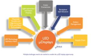
While LCDs and OLEDs are built using thin film area processes, LED displays have been developed based on using single individual LEDs. These LEDs have to be put into position, with missing or defectively connected LEDs meaning a ‘dead pixel’. This kind of defect is less and less acceptable, and, as we pointed out out in another recent Display Daily, (What LED Has to Do to Be Truly Disruptive) to make an UltraHD TV takes 24 million LEDs.
Most electronics assembly is done using pick and place machines. As an excercise, Dr Virey calculated how long it would take to create a display using a traditional pick and place machine that put in a single chip at a time. He calculated that it would take up to a month to make a single display! That means that to build a commercial display, you have to use some kind of ‘massively parallel’ pick and place technology and a range of different concepts are being explored including printing and all sorts of peeling and methods using flexible substrates. This kind of system might take every nth LED so that the LEDs are spaced much further apart on the display than they are on the manufacturing wafer.
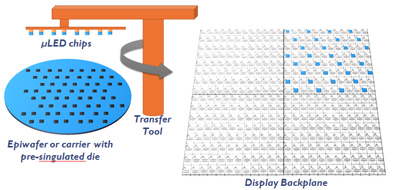 One method is to make individual LEDs & place them. Image:Yole
Although apparently a simple problem. a display specialist at a major semiconductor company that I know told me that it had decided that the pick and place challenges in microLED were such an issue that they decided not to get involved.
If Pick & Place is tricky, don’t do it!
A second approach avoids the pick and place problem by creating the LEDs on a semiconductor wafer (typically CMOS silicon) that contains some circuitry and acts as the substrate. A whole array, as manufactured, is used as a monolithic display, without the LEDs being individually separated out.
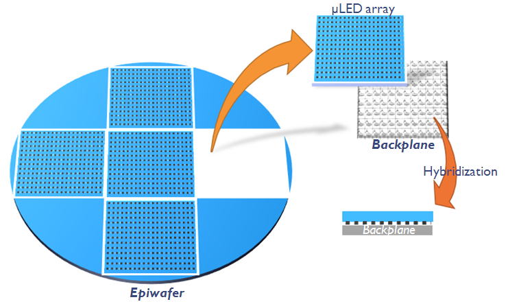 The alternative is monolithic manufacture – which may be OK for small displays. Image:Yole
Limiting to a smartwatch size display reduces the number of LEDs that have to be placed and the area that they have to be placed in and Virey said that he thinks that small displays might be made in a ‘couple of operations’.
Smartwatches also benefit from fine pitch of 200 or 300 ppi and that can also be an advantage as other technologies such as OLED start to get harder at very small pitches. Getting the pitch down also makes it easier to get into near-to-eye applications.
The microLEDs can be very small – down to 10 microns or even smaller. Devices as small as 5 microns may even be possible and desirable, Just to help get a sense of scale, Sony’s Cledis display, which has impressed so many from Infocomm to ISE, has a 30 micron device with a wide pitch of 1.2mm. Of course, LEDs are semiconductors, so the smaller you can make them, they cheaper they should become and the individual LEDs do have to become very cheap.
Defects Can be an Issue
However, going down to very small sizes, which is also essential to keep cost down, means that manufacturing defects that are not an issue on normal LEDs can become a problem when the device is small. If you are making a device that is, for example, 300 microns square, a defect of two or thee microns makes little difference. If you are at 5 microns for the device size, such a defect becomes a killer. Defects that are not killers may still cause too much variability in output.
That means that the LEDs are unlikely to be made in regular LED fabs, but may need more stringent clean room environments. However, Virey does not believe that this is an insurmountable problem, just another issue to be solved. One way that it might be solved is to build in some kind of planned redundancy, although that means more devices and doesn’t help with the cost challenge.
LEDs suffer, as do most semiconductor devices, from issues of variable performance. Traditionally, one of the great skills of the best makers of big LED displays is in matching the LEDs or compensating them so that the output matches. This is also likely to be an issue in microLED displays – the LEDs can differ in colour and in brightness. One of the ‘tricks’ that makers may try is to differentiate between ‘inter’ display matching and ‘intra’ display matching. That is to say, if you select the LEDs for performance, you may be able to group LEDs in the same range within a single display, even though the final result may be different from another display. A traditional LED may come out of manufacturing with ±4 or ±6 variation, while for a display you may want a maximum variation of ±1 to ±3.
One of the ways of helping with colour variability is to use a single colour of LED and then use colour conversion such as quantum dot technology. (That’s a topic we plan to return to)
OLED tends to suffer from some of the same variability issues as LED and so there are driving schemes and technologies that have been developed to help with uniformity. The good news, according to Yole, is that the TFT backplane for a microLED display is ‘essentially identical’ to that used for OLEDs.
There are still many MicroLED challenges. Image:Yole
A/R & MR, but Not for VR?
The fast response time and high efficacy make LED an attractive prospect for near to eye displays, such as those used in VR and A/R. However, VR headsets block ambient light, allowing the eye to work at quite a low level and so display brightness doesn’t have to be very high – it may be just 80 cd/m² or 100 cd/m²
That makes OLED more attractive. However, when it comes to A/R or mixed reality applications, a lot of brightness is needed, so microLED is a natural choice, probably the only choice as for some applications, because of high ambient light, but also significant potential light loss in some of the optics. As a result, some makers are looking for up to 100,000 cd/m².
Turning to the geographies where development is being done, both Europe and the USA have significant development efforts going on and there are also a number in Japan, China and Korea. However Virey told us that Taiwan may be in quite a good position as it has good semiconductor knowledge, an LED industry and also a solid display industry. ITRI is involved and there is work going on to develop a microLED consortium.
So, How Many and When?
Given the range of challenges still to be overcome, it looks as though it will be 2019 or so before a practical product using a microLED comes to market. In 2020 and 2021, the markets will mainly be smartwatches and A/R and M/R headsets, Yole believes. However, by 2021, the technology will start to get into tablets and smartphones and even into notebooks, TVs and monitors.
In the longer term, smartphones will be the biggest segment, by a long way. I know I would like a smartphone that delivered really great colour, enough brightness for easy operation in daylight and long battery life!
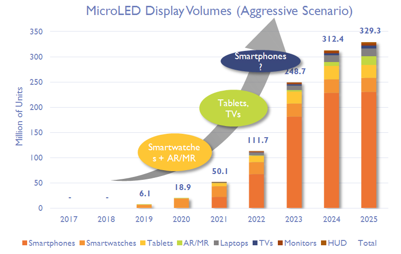 Note that this is Yole’s ‘Aggressive’ Forecast for MicroLED