 Dr Brian Hsieh is from Applied Materials which makes equipment for high technology markets and is now 50 years old. It makes semiconductor equipment as well as display equipment and generated $2.1 billion in display orders in 2016, although it’s a relatively small part of all of its business. The firm makes a number of different equipment types for deposition, testing and encapsulation.
Humans are visual creatures, Hsieh said, ‘seeing is believing’ and the display is a window from the human to the information universe. The last 20 years was the “LCD time”, based on the scaling up of the size of substrates. As a result of that scaling, cost came down a lot. From 2008, the focus changed from simply driving cost down to performance with touch and high resolution coming to the fore as well as LCDs becoming thin and light for smartphones. OLED is increasingly becoming important. We live in a 3D environment and in the long term, Hsieh believes that 2D is not good enough – eventually ‘natural’ 3D will be introduced.
In the Applied Materials roadmap, the three key factors are resolution, form factor and size. Resolution is still going up and displays for VR/AR will get to 2500ppi and even smartphones will get to more than 700ppi. Form factors will move to curved and rollable/flexible configurations. Sizes will continue to increase, TVs going to 70″ and smartphones to more than 5.5″.
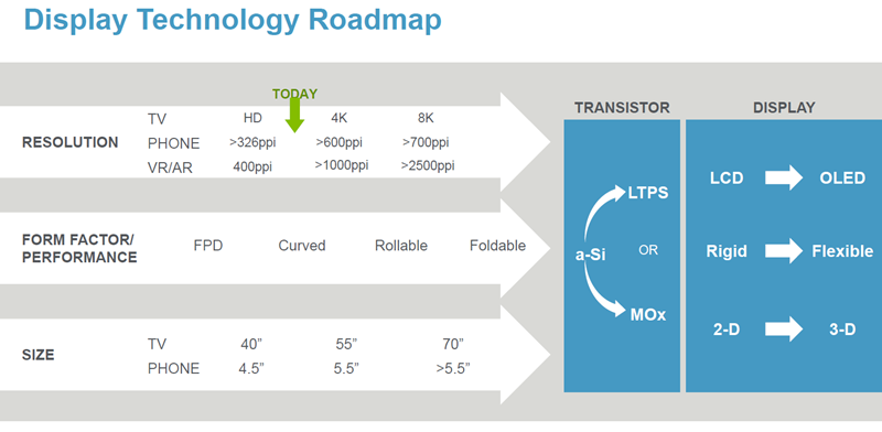
Transistors on displays will develop from being based on amorphous-silicon to metal oxide or LTPS manufacturing as the demands for better quality and features continue.
Hsieh said that in a broad sense, there will be a replacement of making displays from components to making them by process – e.g touch was originally implemented using touch panels, but has shifted to in-cell touch and the change from components to process needs material innovation.
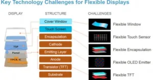
The key challenges in making flexible displays will be in covers, touch and encapsulation. Of course, as ITO is not flexible, ITO-based touch sensors are no good – there is a lot of innovation that is needed still. The cover window for flexible and foldable displays are still a real challenge.
Flexible emitters still need to be fully developed.
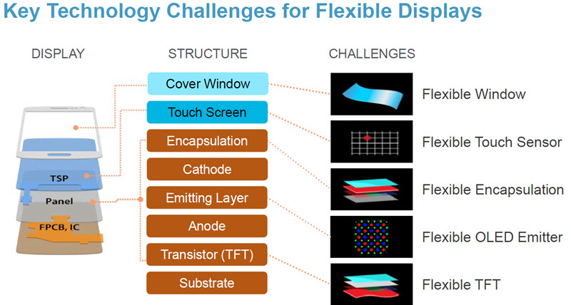 There are still a lot of flexible technology challenges
Applied Materials thinks that the switch to more focus on processes will mean that display making will increasingly look to the semiconductor industry for ideas. In semiconductors – wafer sizes kept increasing but have now ‘maxed out’, but when this happened, device structures and materials changed to keep innovation going.
LCD has been similar – initially substrates scaled up in size, but now there are changes to the details of processes and the use of new materials
Yield challenge is a big one as you go for these higher resolutions because more transistors in an area means more chance of ‘killer’ particles, so more resolution hits process yield. There is a need to look at 8 micron particles and overall getting smaller and fewer particles becomes much more important. How do semiconductor makers address this problem, Hsieh asked?
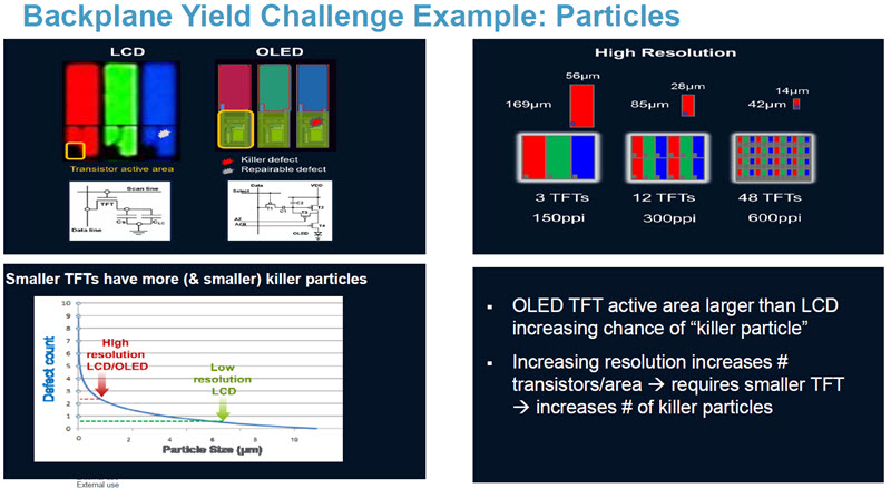 Backplane defects that are OK at low ppi become killers at high ppi
“You can’t fix what you can’t see”, is a phrase that is often heard in the chip business, Hsieh said, and to address this, Applied Materials developed an in line scanning electron microscope (SEM) for chip makers. Once chip makers got to 1 micron features, they needed SEM to deal with defects. There has been much analysis of this size of defects in the semiconductor industry. Now the display industry is approaching 1 micron design rules – so the same kind of understanding of defect reduction is going to be needed by display makers.
The big change, Hsieh said, was to to in-line SEM without destruction and with high throughput. In-line SEM will bring advantages to displays by allowing the identification of defects to find the sources.
OLED frontplanes are a big challenge – it’s a complex manufacturin system to make these, with many chambers involved and lines are typically 100 m long, ‘like a factory within a factory’. New yield management technology is needed and a lot of work needs to be done to bring this to displays.