Axus Technology (Axus), a leading global provider of CMP, wafer thinning and wafer polishing surface-processing solutions for semiconductor applications, announced a partnership with Compound Photonics US Corporation (CP, also known as CP Display), a leading provider of compact high performance microdisplay solutions for Augmented and Mixed Reality (AR/MR), to accelerate sub 5 µm pixel microLED development to the mass market.
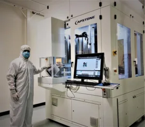
Axus and CP are partnering to integrate critical wafer-scale processes needed for mass-production scale up of CP’s 2 µm pixel, 1080p microLED displays for the next generation AR glasses. Specifically, Axus will deploy its state-of-the-art Capstone™ CMP system with integrated post-CMP clean to enable wafer planarization and surface preparation process solutions for successful wafer-scale bonding of microLED wafers to high-performance CMOS backplanes.
To accelerate development, Axus and CP will set up in CP’s MicroLED Innovation Center for Augmented Reality Acceleration (MiARA) located in Chandler Arizona. The approximately 15,000-square-foot, Class 100 clean room facility provides the infrastructure for Axus, CP and other capital equipment suppliers to conduct advanced process development in Silicon Desert within proximity to global leading semiconductor manufacturers.
Axus’s advanced CMP processing capability is key to enabling CP’s proprietary, small pixel, epi-substrate agnostic microLED integration process scheme. The Capstone CMP system provides the repeatability over multiple wafers and planarity performance within die/wafer to reliably enable bonding of multiple-million micron scale electrical contacts between microLED and CMOS backplane wafers. This addresses a critical mass production process requirement for consistently yielding microdisplay modules with required visual uniformity, which is needed for compact, low power, high brightness AR/MR near-eye applications.
Axus and CP have collaborated since early 2020 to develop wafer-scale bonding process integration between microLED array and CMOS backplane wafers. Today’s announcement further demonstrates the leadership commitment from both companies to advance microLED display fab processes and integration.
Dan Trojan, President of Axus Technology, commented, ”Given the tremendous growth potential and exciting technological advances associated with microLED development and commercialization, I’m very pleased that Axus Technology has the opportunity to support many, if not most, of the technology companies working in this area. Axus is the leader in CMP-related advanced technology and process innovations to enable microLED and its solutions. With the introduction of our new, state-of-the-art Capstone™ CMP system, we also now offer the equipment best suited for implementing such processes in R&D, pilot production, and high-volume manufacturing applications. We’re thankful for the opportunity to continue, and extend, our relationship and interaction with Compound Photonics, which we recognize as a leader and pioneer in this exciting field.”
Peter Wrschka, Process Technology Director of Axus Technology, added, “The synergies between Axus and CP will yield display devices of unprecedented speed and performance. Axus offers years of experience in the surface preparation for wafer bonding and subsequent substrate removal, which is needed to successfully build the next-gen miniature displays. The partnership will significantly shorten the time-to-market for monolithically integrated microLED displays.”
Julie Chao, Product Development Director of CP Display, commented, “We are thrilled to work with Axus to develop CMP and cleaning solutions that enable bonding CP’s CMOS backplane to any sub 5 µm pixel microLED wafer. By working together in MiARA, process improvement cycles are naturally accelerated. This is imperative in meeting the market schedule from developers to end customers.”
MicroLED is continuing to emerge as the most potential display solution to meet the critical requirements of AR/MR applications. Innovations in manufacturing process are critical in enabling cost reductions and volume productions for AR/MR headset commercialization.
About Axus Technology
Axus Technology is a recognized industry leader for equipment and process solutions for CMP, wafer thinning and wafer cleaning applications. Axus enables companies of all sizes from startups to high volume manufacturers to test, develop and implement leading-edge solutions, particularly for novel and emerging materials, process integration schemes, products and applications. Equipment solutions include low cost-of-ownership entry-level tools to state-of-the-art high-volume manufacturing systems. Process testing, development, optimization and scaling are supported by our process applications lab and foundry, which includes a full array of process equipment and supporting metrology, staffed by the most experienced team in the industry.
About Compound Photonics
Compound Photonics (CP), also known as CP Display, is a leading provider of compact high resolution microdisplay technologies. CP’s microdisplay solutions are optimized to serve the augmented reality and mixed reality markets where high performance, small form factor, and low power consumption are most critical. Compound Photonics’ microdisplays enable engineers to innovate and create game-changing consumer and industrial products that can greatly enhance people’s productivity and lifestyle.

