I was very interested to see that Applied Materials (Applied), a key supplier of equipment to the flat panel display industry, was planning to speak at the DSCC AR/VR event this week about developments in optics. I have said for years that ‘There’s no Moore’s Law for optics’, but new optical approaches are coming that do use the equipment that has helped maintain Moore’s Law progress. However, Applied had another topic, microLED, that surprised me.

So, I’m planning to come back to the idea of better optics using semiconductor making equipment in another DD. For today, I want to focus on this new approach to microLED manufacture from Applied.
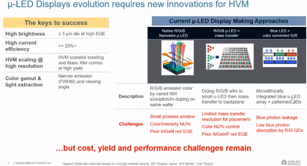
Before starting. the company looked at a range of options in making microLEDs, but it saw downsides to each approach.
-
Nanowires are interesting, but need very accurate doping to generate different colour light in the nanowires and this is ‘a difficult science project, although soluble’, Applied believes
-
Mass transfer of RGB LEDs. This is feasible, but the firm anticipates severe issues in dealing with failed pixels and other defects.
-
Blue LEDs with colour conversion (more shortly)
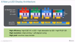
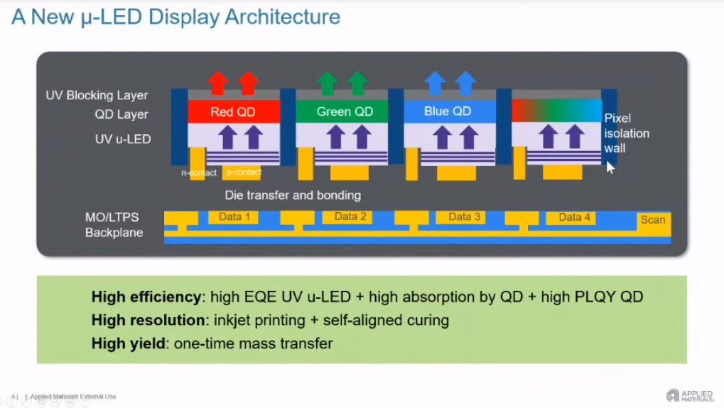
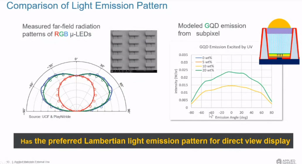
So, having looked at the issues, the firm chose to use UV LEDs. One of the key reasons for this is that it has also chosen to adopt QDs for colour conversion. LEDs are notoriously difficult to make with consistent colour and the colour also varies according to other factors including the drive current and temperature. QDs, on the other hand, produce very pure colours with consistent wavelengths. The normal approach to making displays with QDs is to use blue LEDs with red and green QDs for colour conversion. The challenge with that is that not all the blue light is absorbed and some leaks through the red and green pixels, diluting the purity of the colours (a factor in the failure to develop QD filters in LCDs, so far). Blue light can also cause human vision issues and concerns.
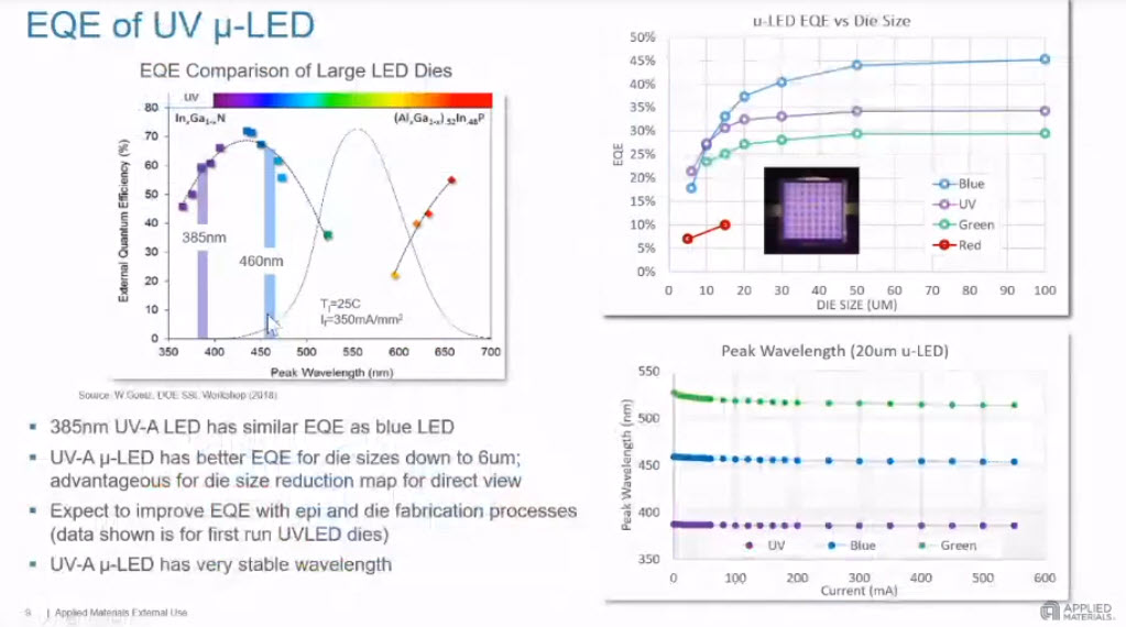
For this reason, Applied chose to use UV LEDs and red, green and blue colour conversion by quantum dots. It found that the EQE of 385nm UV LEDs is almost as good as blue, but it’s very stable at different currents (see chart above) Now, there are no commercially available blue QD materials, as far as I (or Applied) know, but the firm was able to identify a source of cadmium-free materials for blue QDs. It found that it can get very good absorption of the UV for all three of the colours, so that was one challenge overcome.
One Challenge Down, More to Come
However, there is also a challenge to make the pixels and shape the materials. Of course, Applied knows a lot about making semiconductor-like structures and had a really good idea. First the company has designed each pixel to consist of four sub-pixels. Each of them is designed with ‘walls’ to contain the QDs above the UV LEDs. Manufacture means printing the QD material into each of the ‘buckets’ and then applying a high current to the UV LED under each sub-pixel which ‘cures’ the QD so that it solidifies. Using a printer avoids a number of steps and has the advantage that if some of the QD material of one colour goes into the wrong sub-pixel, most of it will not cure and will be removed by washing after each deposition step. Further, after manufacture, Applied can scan the sub-pixels and if one is particularly weak, it can use the fourth sub-pixel to choose which colour to deposit to fix the issue. That improves yield (and this kind of strategy is shared by others that are looking at colour conversion for microLEDs).
Now, inkjet printing has long been touted as a breakthrough technology for display material deposition, especially for OLEDs, but has not been able to match what photolithography has been able to do. Applied’s ‘buckets’ (my word) can really help and Dr Nag Patibandla said during the conference that the firm has made demonstrators up to around 400ppi but is in the process of validating designs up to 1600 ppi in RGB colour, using inkjet printing. Limitations in the print head gantry have been a challenge but the firm has a solution. He even suggested that using ‘another technique’ (not inkjet), the firm could get up to 3400ppi. The firm is developing high volume (manufacturing scale) printers.
The current demonstrators are quite low brightness (for an AR display) of just 1,000 cd/m² but this is said to be a limitation of the backplanes used for the demonstrators and not a fundamental problem. The brightness can be of at least the same order as other microLED microdisplays.
Once the pixel has the conversion layers in place, other processes such as adding coatings to the walls of the container or adding a microlens on the top can be used to improve the collimation of the light coming out, which is important for coupling the light into the optical system (as the initial application is in AR and VR headsets and those will have optical systems to deliver the image to the eye).
Applied is an equipment maker, so it doesn’t plan to make displays itself, but to develop the equipment and license its technology and know-how to others. Based on strong interest so far, Dr. Patibandla suggested that the technology might be in a marketable display by the end of 2023.
So, it’s going to be another time before I get back to the topic of optics. There were several very interesting talks at the event, so I’ll be back with more. In the meantime, the presentations are online for a while and you can register (paid but a reasonable price) via DSCC. (BR)
Peter Palomaki has just pointed out to me that he gave some info on the Applied Materials approach in his SID QD round-up. Doh! (but in my defence, SID is always a ‘drinking from the firehose’ time!) Quantum Dot Round-up at SID Display Week 2021