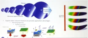
Fabrication of blue and green LEDs – whether for conventional LED signage or emerging microLED applications – has typically started with a GaN epitaxial layer on sapphire. But the limited size of sapphire substrates and the lack of wavelength uniformity may make this approach too costly for microdisplay applications. Allos Semiconductor and Plessey Semiconductor have now developed a GaN-on-Silicon solution that they believe address these concerns.
One of the big advantages of GaN-on-silicon is the larger substrates that can be used. Allos is currently offering 200mm wafer and Plessey says it can offer up to 250mm wafers offering much larger areas than the largest sapphire wafer at 150mm.
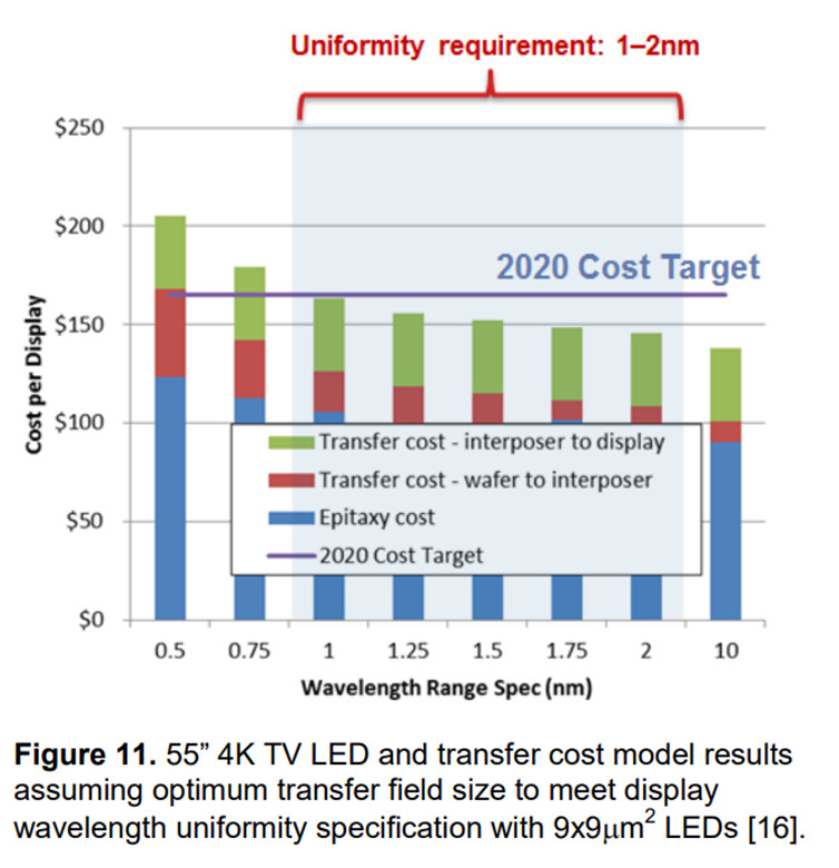
A big yield driver with sapphire is wavelength uniformity. The wavelength variation requirement for LED-based displays is 1-2nm but most wafers have much higher non-uniformities. That means that testing and binning is needed to get the right LEDs to make a display. (One of the key issues in building large SMD LED displays)
Allos Semiconductor has worked with MOCVD equipment provider, Veeco, to show how they can now achieve such uniformities using Veeco’s Propel single 8” wafer machine. For higher production rates, planetary style machines are needed. For example, Veeco’s EPIK 700 batch platform can hold fourteen 6” substrates. In a paper at SID DisplayWeek, Veeco said this system can also meet the uniformity requirement along with anticipated defect requirements.
The defect requirements are dependent upon the LED size and the mass transfer block size (donor field). Veeco said that for QHD smartphones the donor field size is 0.92 cm² and the killer defect size is approximately 1 µm, whereas for 4K TVs the donor field size is 10 cm² and the killer defect size is approximately 3 µm. For both applications, EPIK is capable of achieving over 90% yield.
In paper 45-2, speaker Ajit Paranjpe showed some cost modeling to make a 55” 4K TV using microLEDs. The figure below shows the cost vs. microLED size. He assumes that die are transferred with a stamp of some sort onto an intermediary substrate (interposer) before a number of these interposers are assembled into a TV. But such a process is only possible with extremely high yields for the microLEDs, or if a repair/replace process is in place for bad die.
According to Allos, it is not just the Veeco machines that are responsible for the great uniformity. Their GaN-on-Silicon wafers have specially engineered strain layers that enable two important things simultaneously. Because these layers allow very good thermal homogeneity across the wafer, high uniformity in layer thicknesses (and wavelength uniformity) is achieved. It also allows the processed wafer to remain flat and crack free after cooling down. With sapphire substrates, you can usually have one or the other, but not both simultaneously. Further, Allos said this can scale to 300mm wafers as well, which they hope to prove when 300mm MOCVD systems are available.
Meanwhile, Plessey, which acquired the GaN-on-silicon technology from Cambridge University in 2012, has already introduced a 6” wafer for LED development across a range of market segments. Plessey has also engineered layers to maintain flatness and uniformity over the wafer so it doesn’t warp or “potato chip” due to strain. (Plessey Expands European Reach and LEDs on Silicon Gaining Traction)
They have also addressed another thorny issue with microLEDs. As the size of the device gets smaller, the efficiency drops rapidly. In a talk at SID, Keith Strickland said they have made microLED down to as small as 1 micron. They have seen the external quantum efficiency exceed 20% on devices as small a 4 microns. He said this is partly due to a vertical LED structure. (see the keynote for more on this KN03 Nanorod LEDs Could be the Future)
Plessey with now working with Vuzix to make displays for augmented reality glasses (Plessey Shows GaN on Silicon Microdisplay). In his presentation, Strickland said that by August 2018, they plan to have a monochrome display with 1920 x 1080 resolution based on 8 micron pitch and operating at 60 fps. By December 2018, they hope to have a full color RGB display with 960 x 540 resolution with a 16 micron pitch in a 0.7” form factor and with 60 fps operation. Color conversion will be via a quantum dot layer for red and green.
Interestingly, the backplane is specified as SP70 or eSP70, which are from Jasper Display and leverages work done for their LCoS backplanes. Details of the fabrication workflow were not provided. (Jasper is also working with glo see Jasper Display Optimistic About MicroLED Potential)
A Gen II display is planned for June 2019. This will be a 1” diagonal device with 1920 x 1080 resolution and 60 fps operation with a 11.5µm full color pixel pitch. Plessey says the display architecture will be a triad arrangement so it may include some sub-pixel rendering (the sub-pixel pitch is 5.8 microns). DeepSky is also working on a triad microLED architecture which does use subpixel rendering to try to improve resolution. – CC