
We met with Plessey Semiconductor to learn more about what the company is doing in the microLED arena. Their announcement that the company was “launching the first monolithic microLED display” sparked a meeting. What they showed us was more of a proof of concept demo in a HUD configuration.
First, we need to be clear what Plessey has developed: GaN-on-silicon technology. (Plessey Attacks Monilithic MicroLED Target) That means they GaN on silicon using an MOCVD reactor instead of sapphire or SiC substrates (or bulk GaN). This naturally creates a problem with lattice mismatch and thermal expansion issues which can delaminate or generate significant imperfections in the GaN material. Another problem is meltback etching which can lead to 3D defect and poor yields.
According to CTO, Dr. Keith Strickland, these are the problems they have been working on and they now feel confident that they have this under control and can start to move forward in commercializing the technology. While they are a semiconductor company and can make the LEDs on the GaN substrate, this is not a display. In the monolithic microLED approach they want to take, the wafer must be bonded to an active matrix backplane to drive each LED. The silicon carrier is then removed. Plessey needs partners to do this part.
Strickland said that their main business will be to license their GaN-on-silicon technology but they will build displays as well to prove out the approach. He says that GaN-on-Silicon is the only technology that can address all the production challenges for MicroLED displays in high volumes. Why? He thinks that pick and place or mass transfer techniques will be too difficult as LED emitter sizes get into the 10s of microns range, and it has to be extremely reliable – i.e. not pixel defects can mean five or 6 “9s” of quality control.
Of course the monolithic approach is best for small sizes LEDs with high density in small form factors. That means they are best targeted right now for AR/VR/MR and head-up display (HUD) applications.
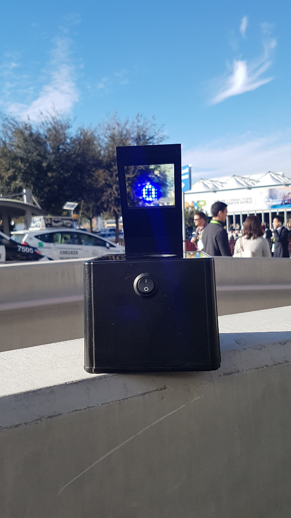
To demonstrate where the company is at this stage, Strickland brought a little demo to show. This was a 5 x 5 matrix, with each element an 8×8 block of 20 micron diameter microLEDs. It was not on an active backplane so driven very simply allowing only the 25 elements in the matrix to be addressed. The picture below shows the HUD type demo with the blue-light projected on a combiner. Note that this is outdoors at Las Vegas so a bright ambient. The LED light is clearly visible and draws only 140 mW.
But Plessey and potential partners have work to do. For one, Plessey needs to find a way to deliver address lines to each microLED to make them individually addressable. Second, it needs to perfect bonding techniques to a CMOS backplane to drive the array. Then there are packaging, testing and other considerations – all before one might consider scaling to mass production.
And this only gets you a blue light device. Some method must be chose to add a color conversion material to add red and green pixels. Strickland sees quantum dots and finely milled phosphors as the most likely path to success, but he will need partners in this area as well.
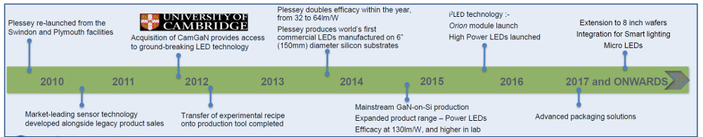
The company has been working with the University of Cambridge since 2010 and is now moving to establish its process on 8-inch silicon wafers.
So, what the company has is impressive, but there is still a long way to go. They can make LEDs as small as 10 microns, but some applications will want even smaller devices. The plan is to show a new addressable architecture by April with a full demonstrator by June. If all goes as planned, display developer kits could become available by the end of 2018.