In 2017, we published a couple of articles about French start-up Aledia, after a talk at the SID Investor Conference and following a trip to the LETI Research Centre in Grenoble. Recently, the company was able to raise cash to accelerate the development of its nanowire-based microLED technology and I had the chance to catch up with President, CEO and cofounder, Giorgio Anania this week.

 The 2017 article from the SID Investor Conference ( gives a background to the technology, but here’s an even briefer summary:
-
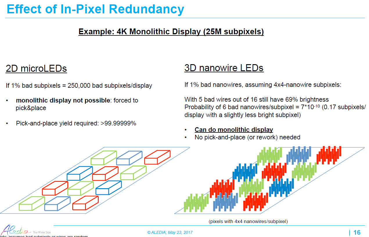
The technology is based on nanowire emitters. This gives advantages of redundancy in emitters.
-
Usually, nanowire length is inconsistent, making performance variable, but Aledia has ‘magic sauce’ that solves that problem (Anania admitted that ‘nanowires are difficult’ and if he was starting again, he might not start from there!)
-
The length of the nanowires can be tuned to make emissions of R, G & B so that a single LED architecture is possible for all three colours
-
The LEDs can be very small and very bright making them ideal for microdisplays and smaller pixels. (they can also be very big)
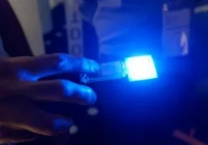
 Aledia showed this big LED in Grenoble in 2017 (Image:Meko). It’s one LED, not an array!
-
The LEDs can be made using standard semiconductor processes on wafers up to 300mm (although work so far is at 200mm)
-
The LEDs can be built on top of CMOS control circuitry.
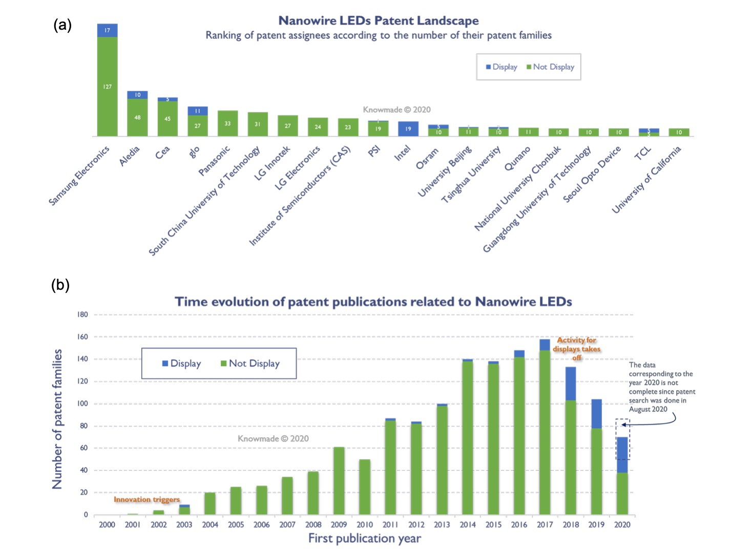
Up to now, the company has been restricted to using LETI and other outside facilities to develop, but the injection of $80 million will allow accelerated development including a new pilot line. In Anania’s words ‘Money changes the execution’ and it helps that his investors include Intel and an unidentified ‘major display maker’. Aledia has been working to develop its technology for eight years, but the problems of limited resources slowing development have clearly been a frustration. In digging around for this article, I found this interesting article on the patent scene for nanowires.
 Click for higher resolution
Anania is quite clear in his mind that microLED will sweep away other display technologies because of the performance and flexibility (in every sense) of the displays that can be made. He also thinks that 2024 is the breakthrough year. (This isn’t the place to discuss this, but I would be less confident about the timescale and certainty.)
The big competition is from ‘2D’ LEDs with traditional architectures, made on sapphire. There are issues that we have previously reported on with this kind of technology when the microLED technology has edges below 10um, especially for red. In particular, the edges become damaged which can cause failure or defective performance. This is not a problem with the nanowire approach which can go down to 3um. Making LED on sapphire poses fundamental problems with defects getting close to the pixel size.
2D LEDs are More Efficient
Optimised 2D LED is fundamentally significantly more efficient than nanowire (80% vs 20%, Anania said), but the nanowire efficiency is maintained as the device gets smaller, while the 2D LED efficiency falls away with size.
At larger pixel sizes, 2D LEDs have an advantage and Anania accepts that in TV, where the pixels are larger and there is more space between them, 2D LED will win over nanowires. Where the microLEDs are bigger they can have higher efficiency and the defects are less significant. Further, the difficult problem of mass transfer is less challenging. On this basis, Anania concedes that 2D will win the battle for larger displays for TV.
However, he is confident that nanowire LEDs can compete for applications including smartphones, notebooks as well as the obvious application in monolithic microdisplays for AR and other uses. The key is getting to 3um pixels. At that size, Aledia believes that the technology can compete with OLED on cost and at that size, mobile applications are very feasible.
Mobile Applications
A key advantage in these applications is that you can get rid of the TFTs on the backplane, using transistors that are made on silicon wafers and attached to the display pixel. (That’s a concept that I first came across with start-up Alien Technology at SID in 1999. That firm eventually moved into RFID where the low cost and tiny semiconductors had a good application). That means much better flexible displays and Anania is very positive about the stimulation that can come from fully flexible displays in notebooks and other mobile devices.
The key to market penetration is cost and Anania believes that there is a simple metric, that 3um pixels can be competitive with OLED for small and medium sized displays.
Turning to monolithic microdisplays, again smaller pixel sizes mean better solutions and being able to make RGB on a single display device are essential for applications in headsets so that you can get away from optical combination of RGB. Anania said that AR is a huge platform revenue opportunity, which explains the interest from Google, Facebook, Apple and others, but it’s a relatively small display opportunity. Nevertheless, Aledia’s technology is relevant because of the small size and high brightness capability.
By chance, competitor JBD released details of its technology this week, (JBD’s 0.13” microLED display in mass production) but I didn’t have time on my call to dig into the competition. However, in the light of the falling number of patents in nanowire technology, I think it’s time I caught up with Gl? et al. (BR)