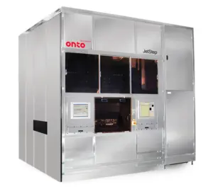
Onto Innovation has recently launched an Applications Center of Excellence, a specialized facility focused on panel-level packaging (PLP) to support the growing chiplet market. This market is expected to see significant growth, with an estimated annual average rate of 103% over the next three years, according to TechSearch International.

Located at Onto Innovation’s headquarters in Wilmington, the center offers a unique opportunity for customers to experience hands-on demonstrations of the company’s hardware and software solutions. These include the Firefly sub-micron panel defect inspection system, the JetStep X500 lithography system, and the Discover family of software. Additionally, customers will have access to systems and processes provided by partnering original equipment manufacturers (OEMs) and materials providers.
The primary objective of this facility is to assist customers in accelerating their technology roadmaps. By leveraging Onto Innovation’s experience and access to next-generation processes and equipment, customers can reduce the time required to achieve production yields. The Applications Center of Excellence is specifically designed to support advanced packaging process development for panel-level packaging, advanced IC substrates (AICS), and wafer-level packaging.
The facility aims to foster collaboration between Onto, customers, and collaborators to develop comprehensive solutions for various aspects of PLP, such as build-up films, redistribution layers, photoresists, copper clad laminate substrates, and glass substrates. By using Onto’s smart factory-enabling Yield Optimizer software, the center aims to streamline fabrication and advanced packaging processes, enabling faster time-to-market for key process steps involved in bringing heterogeneously integrated chips and chiplets to life.

