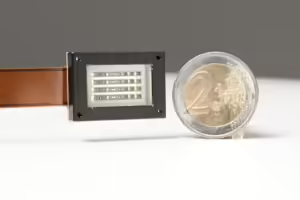
Researchers at the Fraunhofer Institute for Photonic Microsystems (IPMS) have made a breakthrough in transparent electronics by achieving 45% transparency in OLED microdisplays. The team will be showcasing their results for the first time during the International Meeting on Information Display (IMID) 2024 in Jeju, South Korea.
There are two main strategies to achieve semi-transparency in optical systems. The pixel approach involves creating transparent spaces between individual pixels, making it ideal for image overlay in complex optical systems where images are layered between other image planes. The cluster approach groups several pixels into larger, non-transparent clusters, creating larger transparent areas between these clusters. This is particularly well-suited for augmented reality (AR) applications, like smart glasses, where pixel clusters form a seamless virtual image with a micro-optic over each cluster. The transparent spaces between clusters provide an unobstructed view of the real world.
Fraunhofer’s transparent microdisplay technology supports both approaches. The version on display at IMID features the cluster approach, paired with innovative AR optics. The integration of individual pixel clusters into a coherent virtual image is achieved using a microlens array. This optical design allows the setup to be as close to the eye as regular glasses, making it practical for AR applications.

Transparent electronics have been increasingly important in many applications such as ultra-thin touch displays and transparent films used in mobile communications. Until now, OLED microdisplays have lacked transparency, but this new development, part of the HOT project funded by the Fraunhofer Society, could changed that. Initially, these displays achieved 20% transparency, but now they have reached an impressive 45%.

The key to this achievement is the OLED-on-silicon technology, which uses a silicon backplane to house the active matrix drive electronics for the pixels. The organic layer of the OLED is integrated on top, with a semi-transparent top electrode connecting all the pixels. The underlying pixel circuitry is based on silicon CMOS technology, using multiple metal layers, typically aluminum or copper, to link the transistors in the substrate.
A highly reflective bottom electrode ensures optimal optical efficiency, which results in non-transparent pixels. However, as Philipp Wartenberg, group leader of IC and system design at Fraunhofer IPMS, explains, the team achieved transparency by spatially distributing the pixel structure to create transparent areas between the pixels and minimizing the column and row wiring. Additional optimization of the OLED layers, such as avoiding OLED layers in transparent regions, adding anti-reflective coatings, and redesigning the wiring, also contributed to increasing transparency.

