We met up with François Templier of Leti who is working on a new GaN-based hybrid microdisplay. He presented an invited paper at the recent SID that covered the topic and we had planned to meet there, but didn’t make it. I was happy to catch up in Grenoble.
The group is developing the devices for applications that need very high brightness such as augmented reality (which needs to compete with high ambient light and also typically has very inefficient optics) and projection. HUDs are also a potential application. High brightness means really high brightness and the group has already achieved 1,000,000 cd/m² of output.
The work has been going on for around five years and 25 researchers are involved.
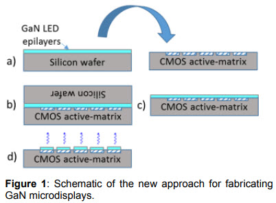
Making ‘monolithic’ microdisplays (i.e. those designed to be used at the manufacturing size, rather than being spread across a large are to create a big display) using LED technology means that as well as the emissive layer, you need a driving substrate based on silicon. One way to make the displays is to make them separately, and then join them together to create the final device.
However, as you get down to smaller and smaller sizes, the alignment tolerances get harder and hard to achieve and that limits the pixel density. 10 micron pixels are probably the smallest that can be made that way, which is a lot bigger than OLED microdisplays at around 3.5 micron. The alternative is to actually make the LEDs on top of the silicon substrate.
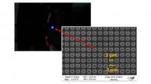
Leti does that by creating a GaN epilayer on a separate substrate, which can be silicon – it doesn’t need to be sapphire. The epilayer is then put onto the active matrix. This has been done on a 200mm wafer already and with pixel pitches down to 3 microns.
There is a hope that full devices will be in production by 2019, initially in monochrome and then moving on to full colour. Phase 1 of the full colour displays may well involve using colour conversion. This will probably be based on semiconductor technology such as a 2D quantum well layer, rather than quantum dots. QDs are unlikely to be suitable for such high brightness. Templier told us that the quantum well technology will be stable and uses the same kind of processes as the LED manufacture. (I seem to remember that Osram has also talked about using a ‘quantum technique’ for colour conversion, but not using quantum dots).
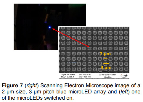
At the moment, the group has made a 873 x 500 resolution 10 micron demonstrator in blue and green and is working with III-V Lab in France as well as Thales, Nokia and the CEA. It is in the process of developing the CMOS controller.