(I enjoyed my individual interview with Ian Jenks but the CEO Forum is also still online).
Although I had been aware of Smartkem ‘in the abstract’ before, I hadn’t registered a key application that the company can drive with its technology (we’ve reported on them 22 times over the last few years). That changed at this SID event. First some background.
Smartkem is a UK-based developer of organic semiconductors that targets the highest possible performance, supported with EDA tools to allow the design of devices. The basic core of the technology is a combination of high mobility (>= 10cm²/Vs) small molecules and low molecular weight polymers, with solvents that allow the material to be applied as ink.
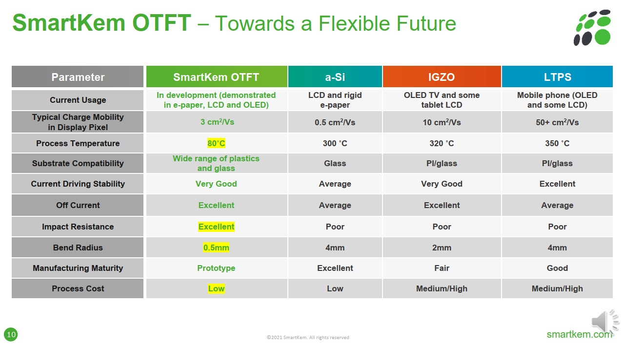
The materials can be processed to high levels of purity which means devices can have excellent electrical stability. The polymer allows inks based on the materials to be deposited on large areas, with good uniformity, Brown said in the Business Conference. Key to the value to the display industry is that the materials, which have off currents in the order of picoamps using the passive interlayers that the firm has developed, can be used on existing amorphous production lines as processes are very low temperature and conventional photolithography materials and processes can be used. The material can be spin or slot-die coated.
Although not as good in mobility as LTPS or IGZO, the TFTs have significantly better mobility than the amorphous silicon used in most fabs. There are big advantages in the low process temperature, off-current (more on that in another Display Daily, shortly), impact resistance and bend radius.
The materials can be used anywhere that a-si is used, but at the show, the company highlighted its use in miniLED backlights.
We’ve covered miniLED a lot, so I won’t repeat the background here, but one of the challenges is to drive the thousands or tens of thousands of miniLEDs. If you only have a few, you can use direct driving and if you need a few more you can use passive matrix addressing, but to do the job really well, it’s ideal to put the miniLEDs on an active matrix (AM) backplane. That’s a challenge.
When you have an AM backplane that is behind and controlling an LCD, the transistors effectively are just controlling the LCD which is like a ‘tap’ (or faucet for our US readers). The light and energy is coming from somewhere else, so the LCD material can be voltage driven and needs only a low level of current as it just has to turn the LC material. The energy to actually create the image is from the backlight. However, once the energy to illuminate the pixel has to come through the backplane, you need much better transistors and more complex configurations as the control of current becomes critical.
That’s the case with OLEDs too, and that’s one reason why OLEDs are made using IGZO and LTPS rather than a-si (and why complexity is much higher with up to 7 transistors for each sub-pixel). IGZO is difficult to make and LTPS is very expensive and tricky to deposit over larger areas (one of the reasons that Samsung’s original plans to make large OLEDs for TVs stalled). It turns out that Smartkem’s material is good enough to allow use for driving miniLED backlights in an active matrix configuration.
Testing MiniLED Backlights
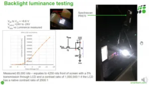
The firm has been doing tests and has demonstrated that it can drive backlights with brightness up to 85,000 cd/m² using a 2T1C pixel configuration. Now, LCDs typically have a transmission ratio of 5% (or less), so a backlight of that level of brightness can give front of screen performance of 4,250 cd/m². (In conversations around our interview, Jenks told me that just for interest, he asked his team to see how far they could push the brightness and they got to several hundred thousand candelas!). Individual LEDs can be driven at up to 100mA (although this level might only be used in small areas in typical content) If the LED gets too hot, it could damage the transistor, but the firm has not done any work to add heat sinking to mitigate this, although it could.
(After the CEO Forum Q&A session, Jenks told me that he thought that Smartkem was the only firm actually using an active-matrix backplane for miniLED at Display Week. I’m not sure that’s accurate, although I haven’t had a chance to check back through my notes. If others did have AM backplanes, they were probably LTPS, which is OK for small demos but would not be feasible for large or lower cost panels)
So Smartkem seems to have a technology that can drive LEDs using the AM manufacturing processes used by current LCD panels. MiniLED may be a really good opportunity for LCD makers that want to compete with OLED, although it would reduce fab capacity by half unless you bought more equipment as you would need two backplanes for each LCD – one for the miniLEDs and one for the LC cell. In the future, however, there is going to be a need to find better ways to drive microLED displays. For example, some of the big LEDs described as microLED and currently being demonstrated are based on a modular approach, using LTPS backplanes. That has to be expensive.
Now, there are challenges. In questions after the Business Conference, the firm confirmed that you need really good conductors to avoid non-uniformity because of the loss of energy across the panel with the relatively higher currents used in driving miniLEDs to this high level of brightness. The company has done some work on this.
It seems to me that Smartkem has also shown that its materials could also be used to make direct microLEDs. I suspect that over then next few years, at display conferences, you may hear more about its Organic TFTs. And that’s without talking about uses in flexible LCDs etc. (BR)
Thanks to Smartkem for releasing this article to be free and to not count towards your free article allowance.


