In April, eLux, Inc. (Vancouver, WA) announced it had achieved two milestones on the road to commercial development of microLED displays, the first being the optimization and automation of its fluidic assembly process.
Before we go any further, let’s describe what fluid self-assembly (FSA) is. The goal is to populate a backplane with microdevices, in this case µLED chips, without using some version of pick-and-place or laser transfer, which can’t transfer the millions of sub-pixels needed for a TV screen fast enough for a viable commercial process.
With FSA, the microdevices are mixed into an ink, and the ink is passed over a substrate that has wells formed into the substrate, with appropriate conductors leading from the wells. As the ink is circulated the microdevices are deposited in the wells.
Part of the eLux announcement is that with a “selective harvest” of µLEDs, the company has produced a 12.3-inch µLED display with a natural yield of 99.987% — that is, 99.987% of wells are populated and function properly before the application of repair strategies.
The second milestone is that “An automated fluidic assembly tool manufactured by an accomplished display panel tool maker is operational in the eLux prototype fab located at Taiwan.”
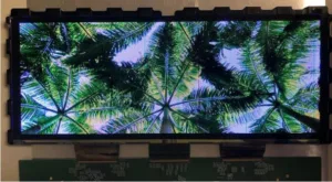
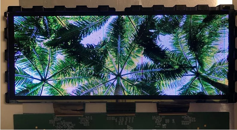 Fig.1 This eLux 12.3-inch demo display containes of 518,400 GaN µLEDs, which were assembled in 10 minutes. (Photo: eLux)
The 12.3-inch demo display (Fig. 1) contains of 518,400 GaN µLEDs, which were assembled in 10 minutes for an assembly rate of 3.1 million devices per hour. The company reports that there were 34 failing subpixels, of which 33 could be laser repaired to achieve after repair defectivity approaching one part per million. Of the 34 defective sites 19 were caused by shorted µLEDs. The company says it must further refine the inspection and selective harvest processes “to produce defect-free displays that do not require repair.”
The new assembly can implement fully automatic cassette-to-cassette fluidic assembly of ten display panels up to 15 inches on the diagonal. Unlike mass transfer equipment, fluidic assembly can be scaled up to substrates much larger than 15-inches, the company says, so tool will be used to develop equipment modules and processes for a proposed Gen 3.5 fluidic assembly tool.
Fluidic assembly randomizes the microLEDs in the liquid, which prevents the mosaic patterns caused by epi-wafer non-uniformity. The technology is suitable for µLEDs sized between 5 and 200 microns.
Older Readers
Some of you, dear readers, may be old enough to remember that 20-odd years ago Alien Technology (Morgan Hill, CA) was developing fluidic self-assembly technology, but their maximum yield of 98% (as I recall) was very far from what was needed for displays. So, what has eLux done to raise the natural yield from two 9s to four 9s?
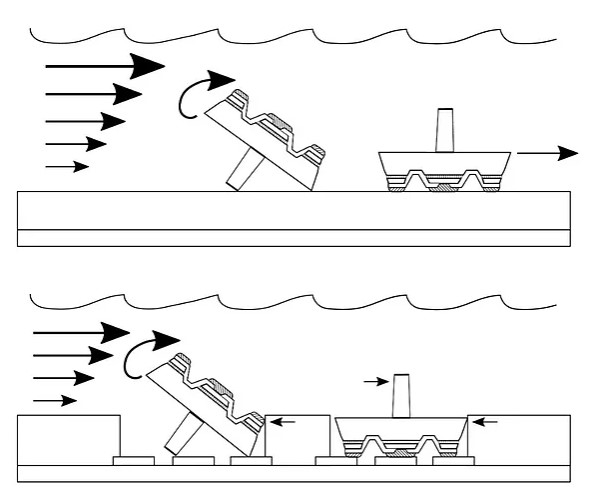 Fig. 2 eLux increases the FSA natural yield by optimizing the orientation and trapping efficiency separately. The uLED orientation is controlled by adding a post opposite to the electrodes. The orientation control is so effective that all uLEDs have their posts pointing away from the glass substrate just several seconds into the assembly process. (Figure: eLux)
That’s the question I asked Jong-Jan Lee, eLux’s President and CEO.
“The biggest different between our work and Alien Technology’s is that we separate and optimize the orientation control and trapping efficiency (Fig. 2). We control the uLED orientation by adding a post opposite to the electrodes. The orientation control is so effective that all uLEDs have their post point away from the glass substrate in just several seconds into the assembly process. Then, the uLED disks are randomly assembled (or trapped) inside the well. The uLED and well shapes are designed to have minimum de-trapping rate. In fact, the de-trapping rate has to be 0% in order to achieve 100% assemble yield. We have achieved the 0% de-trapping rate.
“Alien Technology used “shape matching” to assemble the device, with the trap and the silicon die having matching trapezoidal faces. Devices have random orientation during assembly, so rectangular die are not as efficient as round die. Furthermore, a force is needed to remove a device that does not have shape matching with the trap site. This force is higher than ours and the trap with sloping sidewalls is a less effective trap, so the de-trapping rate is higher than ours. This is the reason we can get four 9s and Alien can only get two 9s. In addition our LEDs are two-terminal devices, and Alien was attempting to assemble more complicated devices with multiple bond pads, and it is more difficult to make multiple connections.”
And that’s why eLux has 100 times the best natural yield Alien achieved.
eLux’s two milestones are impressive. They still have to make further improvements in their natural yield before the process in ready for prime time, but JJ Lee is clear-eyed about that. And, as a fellow µLED entrepreneur told me recently, “JJ is a force of nature.” (KW)
Ken Werner is Principal of Nutmeg Consultants, specializing in the display industry, manufacturing, technology, and applications, including mobile devices, automotive, and television. He consults for attorneys, investment analysts, and companies re-positioning themselves within the display industry or using displays in their products. He is the 2017 recipient of the Society for Information Display’s Lewis and Beatrice Winner Award. You can reach him at [email protected] or www.nutmegconsultants.com.
Editor’s Note
I remember Ken telling me about Alien Technology at the Display Week event in (if I remember correctly) San Jose in 1999, when Sony showed a 200ppi CRT, IBM and NEC had high dot density LCDs (177-200ppi) and Panasonic had a 60″ PDP. Samsung showed a 24″ wide screen monitor and carbon nanotube display. Alien Technology pivoted away from displays and has made a business in RFID. (BR)