Of those things that are accepted wisdoms in the display industry, one of them is that a-Si (the standard backplane for 75% of the display industry) is simply not stable enough to drive AMOLED displays. AUO tried back in 2003 and came up with an RGB demo but ultimately failed. Since, more complex and costly IGZO and LTPS-based backplanes have become the standard for large and mobile displays, respectively.

That convention has been overturned now by the work of a 3 year-old start-up called Mattrix Technologies, a spin out of the University of Florida and a client of mine (IC08 Mattrix is the New NVerPix – with New Switches). As far as I know, this is now a world first – a bottom-emission, white-OLED display with a-Si as the switching transistor. The pixels in this full-color demo are based on Mattrix’s VOLET technology, a vertically arranged three-terminal device that combines the drive-TFT, storage capacitor, and OLED, and a very different approach from the TFT backplane designs used in today’s AMOLED displays.
So, what are the benefits of this technology, I hear you ask? Well multi-fold. First there is a reduced cost for the backplane needed to drive the OLED. The technology uses the cheapest semiconductor process (a-Si), but also radically reduces compensation circuit complexity. Second, the current density in the vertical channel is 2-3x lower, expanding the design space such that lifetime can be improved, or displays can be made brighter. The vertical channel also decouples the current path from the gate-oxide interface, leading to less image burn-in.
Emissive apertures, such as they are relevant in bottom emission devices, are also improved. The technology enables cheaper fabs to be used or built since now expensive high mask backplanes can be replaced with something substantially cheaper. There is less opex in the fab and it allows older a-Si fabs, from Gen 4 to Gen 10, to be repurposed (with a new frontplane) as OLET fabs,.
The Net Present Values (NPVs – the value today of a longer term investment – editor) of greenfield OLED fab projects of all types are also substantially improved. This is a win-win for old fabs and new fabs. Any fab. The technology is a great fit for emissive TV technologies, and for LTPO replacement for mobile applications since you get the capabilities of a lower power display technology with options for refresh rate management.
The “secret sauce” is in multiple areas, from a proprietary nanocarbon source electrode (materials provided by JSR Corp.) to a slightly different driving method and the VOLET structure itself. A cross-sectional picture of the VOLET architecture is shown in Figure 1. Not only is the architecture completely compatible with a broad range of self-emissive materials, from phosphorescent/solution OLEDs, and TADF to QD OLED and QDEL, but a key point is that it can be implemented with existing equipment and processes in all display configurations: both top and bottom emission; WOLED+CF, RGB FMM and RGB IJP.
The demonstrator itself, as shown below in Figure 1 is a 4.7” WOLED panel made by Mattrix on a conventional LCD backplane provided by a Japanese contract manufacturer. It has brightness of 500 cd/m² and resolution of 85 dpi (TV demonstration). The increased aperture ratio of the panel yields a >250% increase in lifetime compared to control OLED devices.
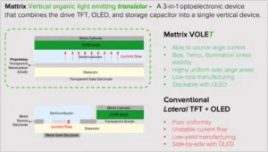
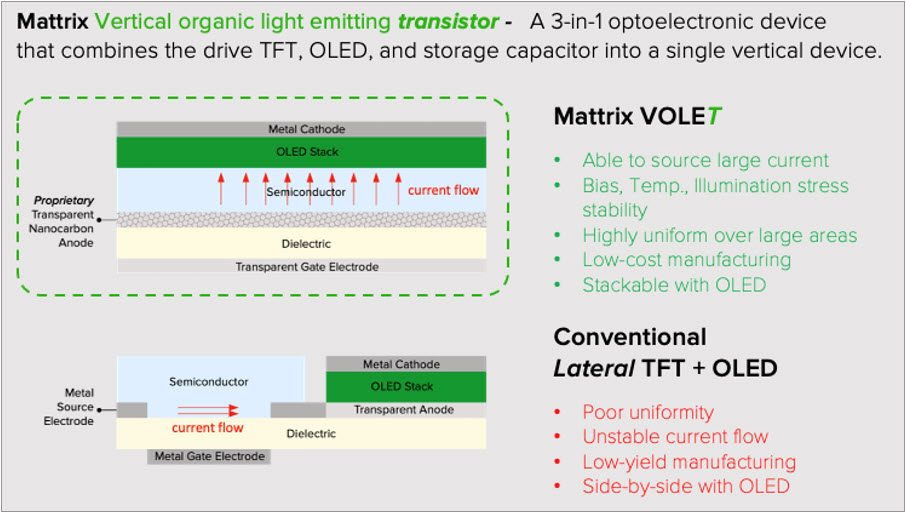 Figure 1: A unique pixel architecture based on Mattrix’s three-terminal VOLET device
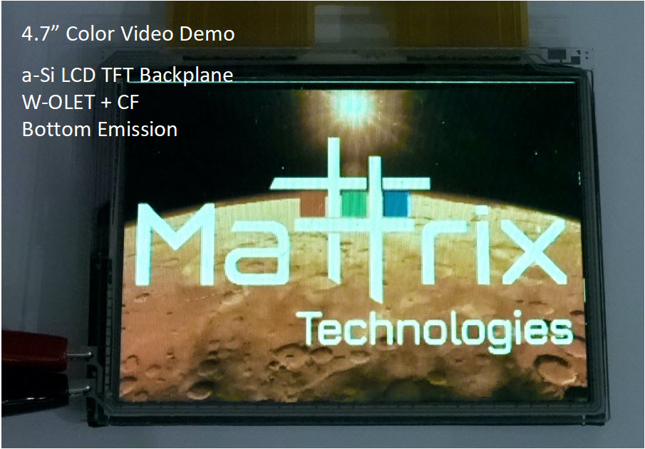 Figure 2: Picture of Mattrix’s AM-OLED Demonstrator
It is remarkable that a demo of this quality can be made on an outsourced, completely conventional, small a-Si line, with off-the-shelf (relatively mid-market, non-proprietary OLED) materials without any mura correction or pixel compensation.
Implications of development of VOLETs
This technology radically simplifies AMOLED production and improves product performance. Up until now, backplane yield losses were, perhaps, 40% of the overall yield challenge in OLEDs: this makes a radical difference as we would expect now a-Si like yields instead in the backplane.
In my view, this technology makes LTPS less important. It makes IGZO less important. It allows companies with only basic a-Si capabilities and older fabs to compete in AMOLED. It radically changes the economics of new and old fabs in AMOLED: as a result, we might expect more AMOLED devices and faster conversion of price sensitive IT categories such as tablets and notebooks. The implications, if it is adopted could be quite industry changing.
Certainly, this is a very interesting development and while mass production may still be some years away, this is something we should all monitor as a new strategic option for the OLED industry. (IH)
This article was moved out from behind the Display Daily paywall by Mattrix, so does not count towards your free allocation of articles.
Ian Hendy is a Display Strategy Consultant based in London, UK. Hendy Consulting provides growth strategy, technology strategy and deal/M&A assessments for players throughout the display value chain. Mattrix is a client of Hendy Consulting.