VerLASE Technologies announces new patent enabling multi-color microLED arrays emitting in green to red, and full color projection, through efficient downconversion of light based on a novel, wafer scale resonant structure around semiconductor Quantum Wells (QWs). The technology replaces phosphors, Quantum Dots (QDs) for color conversion in key applications.
VerLASE Technologies announced today that US Patent No. 9,019,595 has issued on its revolutionary Chromover™ wavelength conversion technology. The technology introduces an entirely new approach for efficiently converting colors from inexpensive, widely available blue/violet light sources such as LEDs or laser diodes to any color in the visible range; for example, to the optimal greens and reds needed for the ideal projection of images, which have been otherwise proven very difficult to create. Significantly, not only can color be tailored but also its spectral characteristics, such that the output can be designed to be a laser, LED, or in-between, in a single color or a RGB projector light source, or as a multi-color micro-array, ideally suited for integrating with microLED displays for the next generation of Near Eye Displays, including holographic 3D variants.
Whether focused on head mounted displays (HMDs) for virtual reality in gaming or augmented reality for the enterprise market, Near Eye Displays (NEDs) have captured recent attention with Facebook’s $2 Billion acquisition of Oculus VR, Google’s $542 Million investment in Magic Leap, Apple’s acquisition of LuxVue, Intel’s investment in Vuzix, and Microsoft’s announcement of HoloLens™ and acquisition of related IP. NEDs and their associated systems and software offer people exciting new ways to interact with computers, mobile devices and their environment. A key challenge, however, surrounds the light sources needed for realistic color projection of images onto a person’s field of view, whether superposed 2D or full color 3D holographic images.
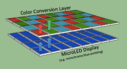
Most microdisplays used in NEDs today have been OLED displays (organic LED) with major drawbacks in brightness, efficiency, color quality and longevity. Displays based on current microLED technology would be much preferred for their high brightness (for projection in daylight), and high efficiency leading to longer battery life. They can also be micropatterned to individually addressable pixels with high resolution obviating other components for very compact physical forms, but the major problem has been that they are monochrome; the phosphors typically used in converting color in LEDs do not scale well to small size and have various thermal issues. Quantum Dots (QDs), for example, have similar problems.
In contrast, VerLASE has developed a wafer scale, thin film conversion technology consisting of a novel resonator cavity surrounding semiconductor Quantum Wells (QWs). The structure is designed to emit light at a desired wavelength when pumped with a known source, which can be available laser diodes or even low cost LEDs. The completely inorganic resonant structure dramatically increases absorption of the pump light and can withstand much higher optical power density than other approaches. The output can be designed to emit as spontaneous unidirectional light as a LED, to lase in stimulated mode as a VCSEL (Vertical Cavity Surface Emitting Laser) with intrinsically high beam quality, or in-between with tailored spectral properties including control of coherence to mitigate speckle, a big problem in projecting images with lasers.
“Today’s microLED arrays offer individually addressable monochrome pixels without a good solution for color, let alone a VCSEL array with tailored RGB colors,” said Ajay Jain, VerLASE’s Chief Technical Officer and inventor of the technology, adding that “this technology can be readily integrated with microLED microdisplays.”
For microdisplays, a color conversion layer can be manufactured as a passive, pixellated microarray down to resolution significantly less than 10 microns with RGB colors per pixel as needed. Conventional, available wafer scale processes are used to form a monolithic thin film structure that can be readily integrated with active microLED arrays.
The technology further scales to higher powers of interest in applications for image projectors and displays of various kinds, ranging from tiny picoprojectors embedded in cellphones to larger venue projectors, and to edge illumination in flat panel displays. Phosphors used in blue laser pumped projector (BPP) schemes can be replaced, for example, with a higher efficiency, low etendue solution at optimal RGB colors with much better color saturation. The structures are similar, only scaled in size, with the wafers arrayed and diced as needed for convenient integration with available pump sources. Power can be scaled for high lumen, large venue image projectors up to cinema range (30-50 kilolumen) and for higher intensity laser pumped applications such as automotive headlights.
“The technology offers a compelling alternative to traditional phosphors or emerging QD solutions in several applications the Company is exploring with key customers” stated Company CEO George Powch, adding his appreciation to the many collaborators who have helped the Company in its development stage.