Verlase has patented a wavelength conversion technology that it hopes will challenge quantum dots.
Click to enlargeThe new patent (US Patent No. 9,035,344) is based on ‘quantum wells’ (QWs) formed from exfoliated 2D materials. These components have applications in both lighting and displays of all sizes. According to Verlase, they offer ‘a practical way around some of the technical hurdles pacing broader adoption of quantum dots…and traditional phosphors for colour conversion’.
Semiconducting materials, like graphene, grow in weakly-bound crystalline layers. These can be exfoliated into very thin layers. Verlase has been investigating photoluminescent QWs made from nanoplatelets of materials such as gallium selenide, tungsten disulphide and moly disulphide. The materials are quantum-confined structures, directly analogous to QDs but are ‘flat’ 2D structures.
When these materials are excited (with low-cost blue LEDs, for example), they can re-emit or down-convert light into colours that are otherwise difficult to obtain: particularly shades of red, green and yellow.
The material composition and thickness of a QW affects its photoluminescence (as the colour of a QD depends on the material and dot size). QWs, says Verlase, have narrow spectral characteristics, better colours and higher colour saturation than traditional phosphors. They are also said to have better thermal characteristics than QDs. The 2D materials have minimal dangling bonds, so are self-passivated. In addition, they are more stable emitters than QDs.
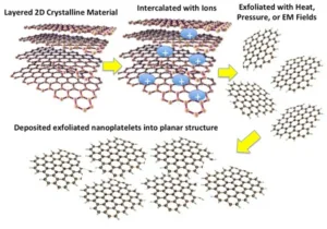
A quantum well can also be formed by sandwiching an exofoliated sheet of 2D semiconductor materials, in air or another bandgap material; alternatively, they can be encased by wider bandgap materials. The sheet forms the ‘well’ region. QWs of 2D materials can be made at a low cost, Verlase has said, by exfoliating 2D crystals grown in a furnace. The exfoliation can be accomplished in multiple ways; one of these is a chemical process. It involves intercalating certain ions between the layers of a 2D crystal, then breaking the crystal apart into its constituent layers in the form nanoplatelets of uniform thickness.
Verlase has demonstrated a roll-to-roll method for laying down 2D nanoplatelets, using a modified Langmuir Blodgett technique – although other methods are possible.
An add-on red-emitting phosphor sheet can be created, producing a warm white white in a conventional SSL luminaire. The corresponding QW sheet, using gallium selenide nanoplatelets, would have emission in the 610-620nm range, and a bandwidth of 30-40nm.
“We believe the unique attributes of 2D QW nanoplatelets can enable the original QD vision of electroluminescent devices”, said Verlase CTO and QW inventor Ajay Jain. Jain added that same basic 2D semiconductor materials can also be used as gain media for lasers and other high value electro-optical devices.