Toray Industries believes it has a major breakthrough in bonding technology for micro-electronic components. The company has successfully developed a new material that enables bonding at significantly lower temperatures and pressure compared to existing technologies. This advancement holds immense potential for applications in electronic components, touch sensors, and other related fields.
The innovative bonding material incorporates Toray’s Raybrid photodefinable conductive material, which is specifically designed for wiring in electronic components and touch sensors. By integrating adhesion technology with Raybrid, Toray has achieved a significant reduction of over 30°C in bonding temperatures, less than half of the levels required by conventional methods. Additionally, the new technology operates under low-pressure conditions, further enhancing its efficiency.
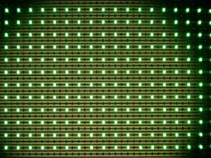
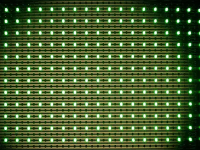
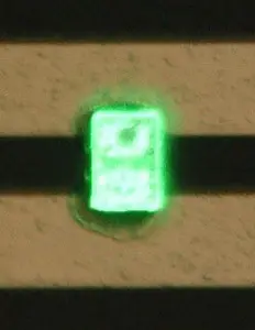
Traditionally, solder and other alloys have been used for bonding purposes. However, they prove to be unsuitable for high-speed mounting due to challenges in miniaturization and the need for high temperatures and pressure. This limitation becomes particularly critical in the production of MicroLED displays, which require mounting of LED chips as small as 10 to 20 micrometers.
To address this issue, Toray has developed a photodefinable carbon paste by combining proprietary nano-carbon dispersion technology with photodefinable conductive paste technology. The integration of carbon enhances the reliability of the bonding process, facilitating secure connections across various applications.
The newly developed bonding material offers several key features:
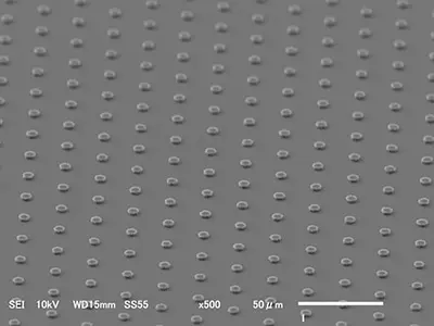
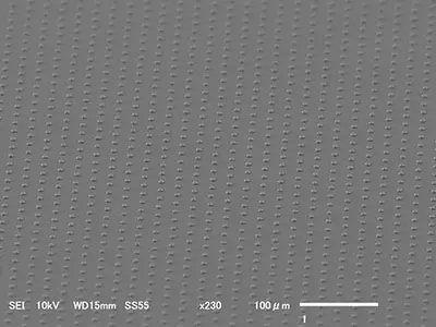
- Fine bump formation: Toray’s technology employs photolithography to create bumps with diameters as small as 5 micrometers. This represents a significant improvement over the previous limit of 30 micrometers, enabling the micro-mounting of MicroLEDs and semiconductors.
- Large-area batch mounting with low temperatures and pressure: Toray’s organic design has reduced the required temperature by an impressive 70°C, down to 110°C. Simultaneously, the pressure needed for bonding has been halved to 5 megapascals. These advancements enable batch mounting of MicroLEDs and greatly enhance productivity.
- Inspection and repair technology: In the event of components not lighting up after mounting, repairs become necessary. Toray’s material enables the laser-transfer of bumps to other substrates, enabling the re-formation of bumps in the repair locations. This addresses a significant challenge in mass production.
To verify the effectiveness of their technology, Toray utilized the mounting and laser transfer facilities of Toray Engineering. Through rigorous testing, the company has established a robust mass production and supply structure for photodefinable conductive materials, developed over the past two decades. Toray plans to leverage the success of its new bonding material to expand its materials lineup and venture into emerging fields such as MicroLEDs and semiconductors.