LGE joined the MicroLED TV club and now there are three members. The announcement provides more insight into the past than it does the future. The µLED TV is composed of segments that are joined together to form multiple size TVs. The resolution grows to 8K and the price to $millions. It takes an army on-site to put it together, uses ~40µm LEDs and reaches up to 1200 nits, so no breakthroughs there.

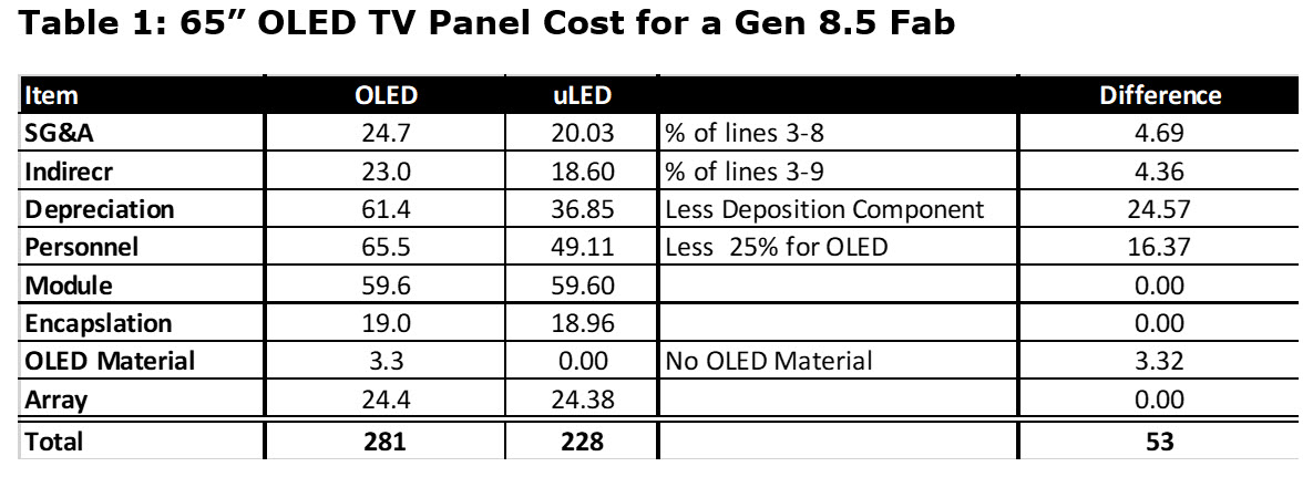
But it does raise the question as to when µLED TVs with <5µm LEDs could reach the market and at what price point? Assuming the challenge of increasing the efficiency of <5 µm LEDs and developing high performance transport equipment would take a while, we selected 2025 as the target date. We projected the cost of a 65” OLED panels based on 2021 figures. Then, we deducted the costs that would not be used to make µLEDs. The savings in this analysis is $53 per panel for a 65” Gen 8.5, but a Gen 10.5 would cut the savings to <$40.
(I asked Barry if there should be a difference in the cost between 4K & 8K as there is a significant difference in yield today, but he said that his assumption is that by 2025, the yields for 8K will be comparable to today’s 4K – Editor)
 Source:DSCC, OLED-A
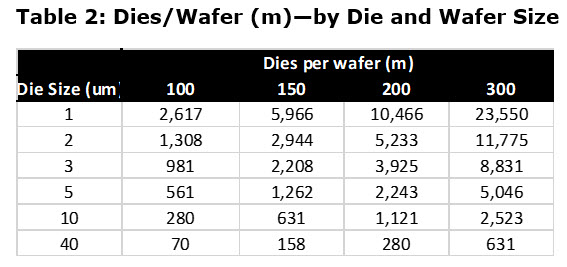
Using this formulation, $53 is left to manufacture 25 million die for 4K or 100 million die for 8K, pick them up from a wafer and place them accurately on a display substrate. That’s what you need to do to meet the costs of an OLED panel. µLED dies are currently produced on sapphire, SiC or Si wafers from 4”-8” in diameter. The vast majority are made on 4” wafers, but a number of companies plan to use 12” (300mm) wafers. The next table shows the number of die that can be produced by die and wafer size.
 Source: Silicon Cost Calculator
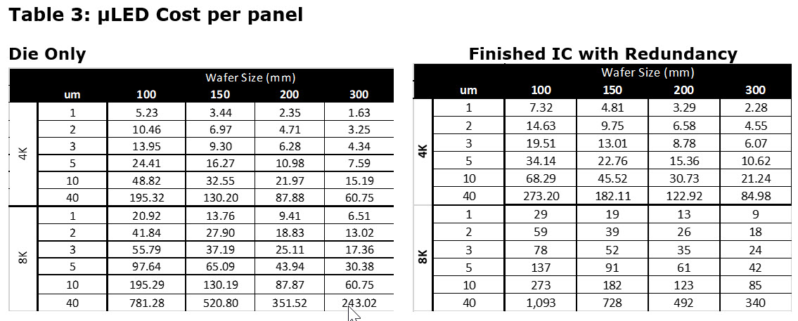
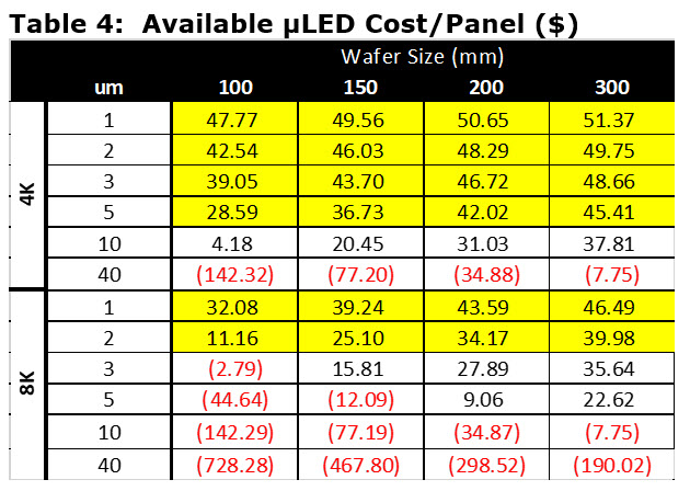
Accounting for yields of 90% and wafer costs of $500, $750, $900 and $1400 for 4”,6”,8” and 12” finished wafers, respectively, the cost per panel for 4K and 8K µLED is shown in the next table. The die must be converted to chips and when transported must absorb the transport yield and the subsequent repair cost. LEDs can suffer from catastrophic failure, so if you use RGB LEDs, you probably need to allow some redundancy to allow for this. If you use nanorod/CNT LEDs failures are less likely to be catastrophic as there are more emitters on each device.
The assumptions made were:
- Wafer Yield 90%
- Chip Conversion Cost – 5% of die cost
- Transport Yield — 99%
- Repair Cost – 50% of the die cost
The full cost of the µLED is shown in the table on the right
 Source: OLED-A
Subtracting the uLED cost per panel from the savings from not using an OLED, provides the available expenditure that can be devoted to mass transport. The saving per panel is then converted to capex, by multiplying it with 900K panels per year and assuming 6 years of depreciation. If the comparison was against the Gen 10.5 OLED fab being planned by LGD, the µLED 8K would be substantially more challenging, leaving only 1 and 2 µm dies as the feasible solutions. In the following tables, yellow signifies feasible solutions.
 Source: OLED-A
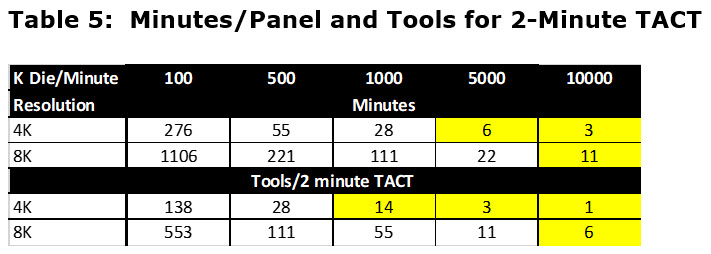
The next table shows the minutes required to mass transfer the dies based on resolution and transfer speed; followed by the number of tools needed to achieve a 2 minute TACT, similar to OLEDs.
 Source: OLED-AThe final table shows the capex available for a mass transfer tool based on the transfer speed and the savings available, after the uLED cost is subtracted from the savings.
Since no mass transfer tools are available for mass production other than Pick and Place, which operates at 400 die/minute, we assumed the capex would be close to the cost of a Gen 8.5 IJP, which is ~$25m. It is likely that the transfer speed will be a minimum of 2.5 million die/minute for 4K and 5 million die/minute for 8K.
There are 10s of approaches to mass transfer, but only three that offer the possibility of more than 1 million die/minute. They are fluidic assembly, laser transfer and micro printing. Speeds have been published but not demonstrated or validated. However, Samsung Display has a prototype environment using the QD-OLED process flow but replacing the VTE deposited blue OLEDs with IJP blue nanorods. The new process could be in production as early as 2024, should Samsung management make the go-ahead decision in a planned review meeting later this year.
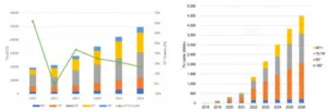
The opportunity for 4K µLED TV is very large. By 2026, the Advanced TV market is expected to reach 50m units (25% of all TVs) and 90% of these TVs will have 4K resolution according to DSCC.
Advanced TV Forecast by Size
 Source:DSCC
An alternative approach is to use red, green and blue µLEDs and eliminate the need for any color conversion. However, the side-by-side pixel design would require redundancy for each pixel doubling the die count. Instead a nano LED design is being developed where a 1 µm die would have up to 50 emitters and all the LEDs use a Carbon Nanotube (CNT) construction with GaN and have the efficacy of blue. These nanoLEDs are being developed by ns Nanotech, Aledia, Gl? (recently purchased by Nanosys) and Porotech. (BY)
Barry Young is the CEO of the OLED Association