
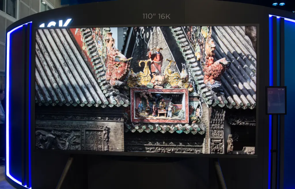
At Display Week 2023 in Los Angeles, the number one LCD panel maker, BOE, showed some very cool products based on LCD technology including a 110” 16K (not a typo – 16 times the pixels of 4K!) LCD that received a tepid reception by ‘the gadget press’. I think they missed the point.
LCD is Now a Chinese Business
As long term observers of the industry will know, the Japanese are almost out of TV panels and the Taiwanese are trying to move their LCD capacity away from TV. Samsung is completely out of the LCD business now, and the gossip at SID was that LG’s remaining fab for TV LCDs is to be sold to Skyworth of China. That would leave just the Chinese (with the Indians joining in). So the field is being left to the Chinese makers, of which BOE is the biggest.
Anyway, BOE had a very good looking ‘UB Cell’ panel that has very high contrast from an IPS panel that uses Merck’s best FFS LC material (as used by LG in its IPS Black panel). It also had a 110” 8K panel with 120Hz refresh that looked great. Although the best LCDs don’t quite match up to OLED in image quality if you are very picky, they give fantastic results compared to the LCDs of just a few years ago. And LCD is what people will continue to buy for some time, because of the vast investment over decades in the supply chain. So LCD is not going away any time soon and the Chinese makers, like BOE and TCL/CSOT which was also at the show, will continue to develop their LCD technology.
The 16K Set and Why it Deserves Respect
Anyway, back to the 110” 16K set… HDTV Test’s Vincent Teoh was quick to put out a video that was pretty ‘meh’ in its judgement on the BOE set. From his point of view as a maven of image quality, I get why he wasn’t that impressed. After all, 400 cd/m2 peak brightness is not that much and the set only had 60Hz refresh. Lots of other posters (including Tom’s Hardware) picked up on his comments. The impression of ‘not much to see’ was not helped by the fact that BOE really wasn’t highlighting the technical achievements, but just showed the panel with a specification list. However, they did publish a paper in the Symposium, but even before I spotted that, I counted myself impressed with the achievement.
If you’ve been around long enough in the LCD business, you’ll know that the limit of panel size is around the 110” mark. One of the reasons for that is the issue of driving the panel. An LCD works by having a different voltage on one part of the subpixel than another. The differential voltage causes the LC material to change its alignment and pass or block the light. That means that to get an accurate image, you have to get exactly the right voltage to the correct pixel at exactly the right moment. However, because of the need to pass the light from the backlight through the LCD cell, you can’t just connect the sub-pixel to a driver chip as you might in, for example, an LED wall. In an LCD, you put the voltage that you want on one side of the pixel into a column driver along the top (or bottom or both) edge, and, a line or row at a time, you then fix the voltage on the other side of the pixel. The current passes down the (very thin and/or transparent) electrode connected to one side, through the TFT and LC material and back through the (very thin and/or transparent) row electrode.
The column driver chips are glued along the top (usually) or bottom (or both) edges and the row drivers are glued down (usually) one side. Frankly, gluing 48,000 column drivers (one for each RGB line) along the top is already quite an achievement!
Unfortunately, the electrodes have capacitance and that is a real fly in the ointment. It’s especially a bigger problem as the frequency of driving the pixels goes up. When does the frequency go up? It goes up when you try to drive more pixels per second, or more importantly, more lines per second. Adding more resolution horizontally doesn’t increase the speed needed (i.e. going from 4K to 8K or up to 16K) because the operation is fundamentally parallel – more pixels simply means more column driver chips. (I’m leaving the second tricky issue, that you have to get the values for the pixels from the host system to the column drivers for another day!)
Designers Want Square Pixels
However, graphic and video system designers typically want ‘square pixels’. That does not mean that they have to be literally square in shape, but that there are the same number of pixels per inch horizontally and vertically. So as your resolution goes up horizontally, if you want to maintain the ‘square pixels’, the vertical resolution also has to go up. On that basis, to make a 16K display, you need 8,640 lines of vertical resolution and you only have as much time as an 8K display at 120Hz (which BOE also showed) or 4K at 240Hz or FullHD at 480Hz. (Each has the same number of lines per second).
So you don’t have much time to load each of the columns (518,400 times each second without any margin for error at 60Hz for 16K). Not only that, as the set gets bigger, the line length between the column drivers and the pixel gets longer and the capacitance goes up. One way to reduce the capacitance is to use a wider electrode, but with 16K, the line width has to be reduced to squeeze the pixels in, so that gets worse. The height of the 110” panel is big so the capacitance also gets worse (and in the past, companies have put source drivers at the top and the bottom of the panel to get around this).
Oxide Helps
One point that worked in favour of BOE is that the panel was made with a TFT backplane using oxide technology which needs less charging time than earlier amorphous silicon TFTs (a-is). However, BOE found that it couldn’t use its best ADS (IPS variant) technology for the panel and had to use another LC mode and that meant that aperture ratio was just >2% – which is why the output is just 400 cd/m2. The best panels can get towards 5% so much more of the light can get through from the backlight.
The final point is that the panel is too big for the transistors to be deposited in a single exposure during photolithography, so the panel is created with multiple exposures. There is always a danger of mura where the splicing occurs but I didn’t spot any real issues with this on the BOE panel.
BOE did provide a technical paper on the development at the Symposium, but if you are not already well up to speed on LCD manufacturing, it’s heavy going. (Session 56.4 C Li Exploration of Ultra-Large Size 16K High Resolution Technology).
Anyway, as far as this writer is concerned, in several ways, this is the hardest to make LCD that I’ve ever seen, so kudos to BOE for continuing to push LCD R&D onwards, even if what they showed did not excite the image quality enthusiasts!
Bob Raikes is semi-retired from the display industry, but still edits the 8K Association newsletter and contributes to Display Daily.