In February a team of researchers from Binghamton University (Binghamton, New York), Blue Wave Semiconductors (Baltimore, Maryland), and Solar-Tectic LLC (Briarcliff Manor, New York) published an article in Elsevier Material Letters reporting “the growth of a crystalline silicon thin film…below 600ºC…with electron mobility of 188 cm²/v•sec….”
The challenge with silicon backplanes has always been the need to process them at a sufficiently low temperature so that standard display glass would not melt or soften. Unfortunately, it is hard to produce silicon pixel switches at low temperature that have good switching characteristics.
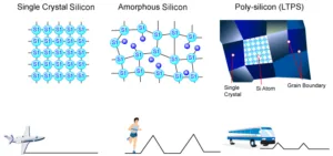
The backplane that appears in most LCDs today is made of amorphous silicon (a-Si). It can be deposited at low temperatures on very large substrates with excellent reliability. Although its switching characteristics are poor, the material has been made good enough for even very large-screen TVs. However, it is not good enough for smartphone displays with high pixel density.
Polysilicon is a form of silicon that sits between the amorphous silicon of low cost LCDs and the single crystal silicon of semiconductor chips. Image:AUO
Enter low-temperature polysilicon. As it generally practiced in the display industry today, a layer of a-Si is deposited and then raised past its melting pointing with an excimer laser. The silicon gets hot but the glass substrate doesn’t. The end result is that the substrate is covered with many crystalline domains. The larger these domains, the more quickly the pixel switches switch. LTPS offers significantly better switching characteristics, but the process is slow, the characteristics of the switching transistors are somewhat inconsistent across the substrate, and it is difficult to use the process on large substrates. The largest LTPS fab today is Gen 6. (Although at Display Week, Coherent, which makes many of the lasers said that it could support G7 – Man.Ed.)
Which brings us to the paper by P. P. Rajbhandari and his colleagues. Nearly a half century ago, S.R. Herd and his colleagues discovered that crystallization of amorphous silicon occurs at a lower temperature in the presence of a metal. This metal-induced crystallization (MIC) has become a standard process in the semiconductor industry. Typically today, silicon is dissolved in an appropriate metal, and the temperature is then reduced until silicon precipitates from the saturated solution. The authors used a variation on this system in which the temperature is kept constant and the silicon is increased until the silicon deposits on the substrate. The authors use thin films of silicon and gold, and they have painstakingly used a variety of analytical methods (XRD, RAMAN, XPS, SEM, and TEM) to prove they have indeed produced crystalline silicon domains.
Their measurement show crystalline domains of roughly 50nm, and a resulting electron mobility 188 cm²/v•sec., which is nearly 20 times that of typical LTPS mobilites on real panels.
The authors conclude that the “high electron mobility…and strong crystalline quality mean that this process can replace LTPS…on large glass substrates (generation 10.5 for displays.
I found myself with some manufacturing-oriented questions, so I arranged to have an email interview with Ashok Chaudhari of Solar-Tectic, one of the paper’s authors.
KW: On what size substrate did you fabricate the material?
AC: About 1″ squared. We made many such samples, and the samples we tested were actually made four years ago and kept in open air (non-sealed box). We should have mentioned this in the paper as it adds to the manufacturability/ commercialization potential of the material.
KW: Assuming that the initial application of your material would be for smartphone displays, display makers would probably want to fabricate on a Gen 6 fab. Do you see any problem in applying these films on such a substrate?
AC: None at all
KW: How variable is film thickness over these dimensions?
We haven’t tried Gen 6 fab size substrates but the cross section SEM and TEM seem promising.
KW: Would the variations be enough to significantly affect display characteristics?
AC: Good point and we would need to investigate this of course.
KW: Can you estimate the relative cost of fabricating your high-mobillty film vs. LTPS and IGZO?
AC: Compared to LTPS which as you know uses ELA [excimer laser annealing], our process is much simpler — the cost should be much less. Not so sure about IGZO as I haven’t compared carefully but IGZO mobility is much less than LTPS and our process and so right there you have a cost difference since performance is less. That would include materials cost and TAC time.
KW: LTPS has sufficient mobility and aperture ratio for fine-pitch displays. Why would a display maker prefer your material?
AC: Because it can grow high mobility films at much lower temperature than LTPS and because we can use much, much larger substrates. In fact, substrate size is only limited by the reactor size.
KW: It seems to me that one advantage of your very high mobility is the ability to fabricate more demanding high-speed circuits on the display substrate? Do you agree?
AC: Yes, absolutely.
Okay. That last one was a softball question and I admit to leading the witness, but I wanted to get the idea of high-performance micro-circuits on glass into the interview.
From a materials perspective it seem the authors have something interesting — but it’s an interesting something on a 1-inch substrate. Chaudhari sincerely believes that depositing and processing the films on large substrates in high volume will not be difficult. But the two-step transition to pilot production and then high-volume manufacturing never ever progresses without problems. This material and process could be important to the display industry. I will track thenm with interest as they leave the laboratory. – Ken Werner
Ken Werner is Principal of Nutmeg Consultants, specializing in the display industry, manufacturing, technology, and applications, including mobile devices, automotive, and television. He consults for attorneys, investment analysts, and companies re-positioning themselves within the display industry or using displays in their products. He is the 2017 recipient of the Society for Information Display’s Lewis and Beatrice Winner Award. You can reach him at kwerner@nutmegconsultants.com.
Solar Tectic has also been developing a ‘Sapphire-like glass’ (Solar-Tectic Developing Material Technologies Having Display Applications – subscription required)