Speckle has been a major challenge for lasers to be used for display systems in laser projectors and used for other illumination purposes. The coherent nature of laser light creates pockets of lights through interference of wavefronts forming a noisy visual effect called ‘speckles’.

Speckles are actually not “things”, but are simply visual effects and the size of the speckles is dependent on the scattering surface that the laser beam falls on, the iris or aperture size of the eye or the camera, etc., and they make the image displayed either not legible or simply not pleasant to look at. The measured parameter of such effects is usually quantified by a measure known as the “speckle contrast”.
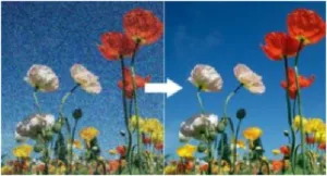
Speckle contrast reduction has become a major task for developers of laser-based systems, in order to make displayed images appear “speckle free”. Figure 1 shows an image with speckles on the left and a de-speckled image on the right. It is obvious that the image on the left is not acceptable and the quality of the de-speckled image on the right is superior.
Speckle (left) vs de-speckled (right) image comparison
Among many known methods in speckle contrast reduction, the most common approach is to use rotating diffusers as shown in Figure 2. The diffuser is used to “destroy” the coherence of the laser light. In reality, the diffuser creates continuous variations in the speckle pattern over time. When viewed by the user, the average of the speckle patterns within the retention period of the eye will be observed, averaging out the speckle patterns resulting in smaller perceived speckle contrast.
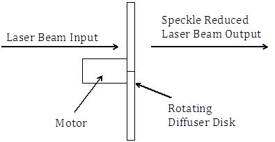 Figure 2 – De-Speckling with Rotating Diffuser
The stronger the diffuser and the faster the rotation, the lower the speckle contrast. On the other hand, a stronger diffuser degrades the etendue of the light source more, which results in lower coupling efficiency into the projection system. In addition, a rotating diffuser for high power applications encounters major problems in heat sinking without having a massive diffuser; such a large diffuser would require a higher power motor, which reduces the reliability of the speckle contrast reduction system.
A new patent-pending speckle contrast reduction system is being developed by Litech International, LLC with a potential of cost reduction and simplified system design using the computing power available from the IC industry. The relentless advance in computing power has been driven by consumer products including mobile phone, computer tablets, gaming devices, graphic devices, etc.
Semiconductor devices, commonly known as integrated circuits, or simply IC’s, have penetrated into every aspect of our lives. Most people are not able to wake up in the morning without the alarm from the cell phone. I have not carried an alarm clock for many years during my travels. Your car does not move without IC’s. There has been a tremendous amount of progress, fuelled by investments in IC developments, equipment making and the whole supply chain in IC making. The major parameter in such development is the Line-Width of connections, measured not in micrometers or microns (?m) anymore, but in nanometers (nm). Line-width is directly related to the density of transistors and the processing power of the IC’s.
As the line-widths continue to shrink in silicon fabrication processes, the number of transistors in each processor continues to rise. Optical wavelengths had been believed to be the limits of the resolutions and line-widths of the smallest features possible. Many in the semiconductor industry had come to believe that features smaller than 1 ?m could not be printed optically. New methods including immersion lithography, dual-tone resist and multiple patterning have continued to improve the resolutions. Meanwhile, current research is exploring alternatives to conventional UV, such as electron beam lithography, X-ray lithography, extreme ultraviolet lithography and ion projection lithography. The line-widths as a result, have gone down to 10 nm and below.
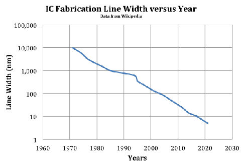 Figure 3 – IC Fabrication Line Width versus Years
Figure 3 shows how the line widths of the smallest features in an integrated circuit (IC) has shrunk over the years from 10 µm in 1971 to the current line width of 10 nm to 14 nm, and continues to shrink to the predicted line width of 5 nm in 2021. Although you might expect this progress to be gradual, the straight-line trend in plot with a vertical log scales says otherwise.
I can’t explain the dramatic progress, but there is a law named after Gordon Moore, the co-founder of Fairchild Semiconductor and Intel, who in 1965, described in a paper that the number of transistors in an IC doubles approximately every two years, the well known ‘Moore’s Law’. I do not think that even Moore expected his law to be true even after half a century.
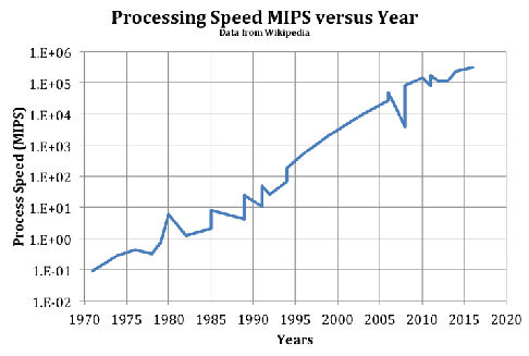
It is, perhaps, even more amazing that the higher density of the transistors together with the higher clock speed has meant that the process power in terms of execution of Millions of Instructions Per Second (MIPS) also shows a straight-line trend in the plot with vertical log scale as shown in Figure 4. There should be a Law on this to be claimed by someone. The progress is not simply ‘natural’ as it is shaped by millions of people and, more importantly, trillions of dollars.
Many of the imaging systems and techniques that we use today, including Light Field Cameras, Spherical Cameras, splicing and combining of multiple digital images, etc. all depend on tremendous amount of processing power. What could not have been done before is possible now. One major push for such development is the need to advance Virtual/Augmented Reality systems with faster response, higher resolutions, wider fields, etc. Such needs, demanded by millions of consumers in every aspect of their lives, have provided the return for the investments needed to attract a large sum of money to solve these challenges. It would be very advantageous if the de-speckling system could get a free ride from such efforts.
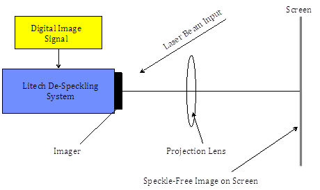 Figure 5 – Functional Diagram of the Litech De-Speckling System using Digital Computing Power of the Processor
Figure 5 shows the functional diagram of the system being developed. When the imager is driven by a laser beam, the image formed and projected onto the screen will be full of speckles, making the images totally unacceptable by any standards. The Litech De-Speckling System is designed to take the digital image signal, process it with the “almost” free computing power of the digital processor, output the signal to the imager, and together with some optics without mechanical movements, a de-speckled image will be projected onto the screen.
Such a system was presented to selected potential licensees some time ago. Initial feedback indicated that the current processing power at that time, might not be fast enough to handle both the Litech de-speckling functions and the standard functions simultaneously, using a single processor for digital cinema applications. If the processing work is done using a dedicated processor, the cost advantages will be defeated. On the other hand, it is expected that for smaller system with non-4K applications, a single processor might have been sufficient using this technologies, even then.
Time has passed. The “straight-line” trend of the MIPS improvements has shown 1,000,000 times improvement in four decades, which equates to about 40% per year. In another few months, the process power will have been doubled since the last study and dual processors will no longer be needed. The computing power of a single processor will be sufficient, then, for running the applications at the same time as handling the standard functions.
This technology is available for co-development and licensing. Please contact Kenneth Li of Litech International, LLC for further details. Email: [email protected].