
Well, I made it through hours and hours of talks about quantum dots and display technology at the first ever virtual SID Display Week! To be honest, there were some things I rather enjoyed about the virtual format. It allowed me to skip things I didn’t want to see and go straight to all the talks of interest. And I did even have a few chat sessions with connections I would have typically met in person.
Of course, I missed the in-person nature of the conference and gawking at the impressive TVs on the show floor, but I found it was well-worth the time to attend this year. Kudos to SID and all of the contributors for putting on a good show in the midst of a pandemic.
Let’s jump right in and I’ll provide you an overview from the three segments of the conference that I usually focus on at SID Display Week. In part 1 I will review the Business conference, followed by Part 2 which will contain my commentary on the technical symposium and virtual showroom.
Business Conference
I will admit I didn’t watch every talk at the business conference, but there were a few important ones with take-aways that pertain to color conversion and QDs.
Sid Mohan of DSCC provided a great overview of the use of IJP in displays. While the idea (and prototypes) have been around for a while, the use of IJP is really quite new in mass produced display products. OLED has found a way to take advantage of IJP for TFE (Kateeva), and we can finally point to commercial IJP OLED panels from JOLED. It seems there is still a long road ahead until IJP becomes common practice for OLED device fabrication (DSCC predicts CSOT/TCL will be producing IJP OLED panels in 2024) but both QLED and OLED have the potential to leverage this powerful technology. QD-OLED especially (expected to come online in 2021) should be an ideal fit for IJP so as to not waste the precious QD inks that are likely to contribute significantly to material costs. Recall that Samsung chose SEMES over Kateeva for this technology earlier this year. DSCC and others have recently started to cover Samsung’s QNED technology. This is something that is still at R&D stage and is (in my opinion) simply something to keep on our radar for now. Once there is a significant demonstration of the technology I will devote some time to covering it, but for now there is more than enough QD technology to talk about!
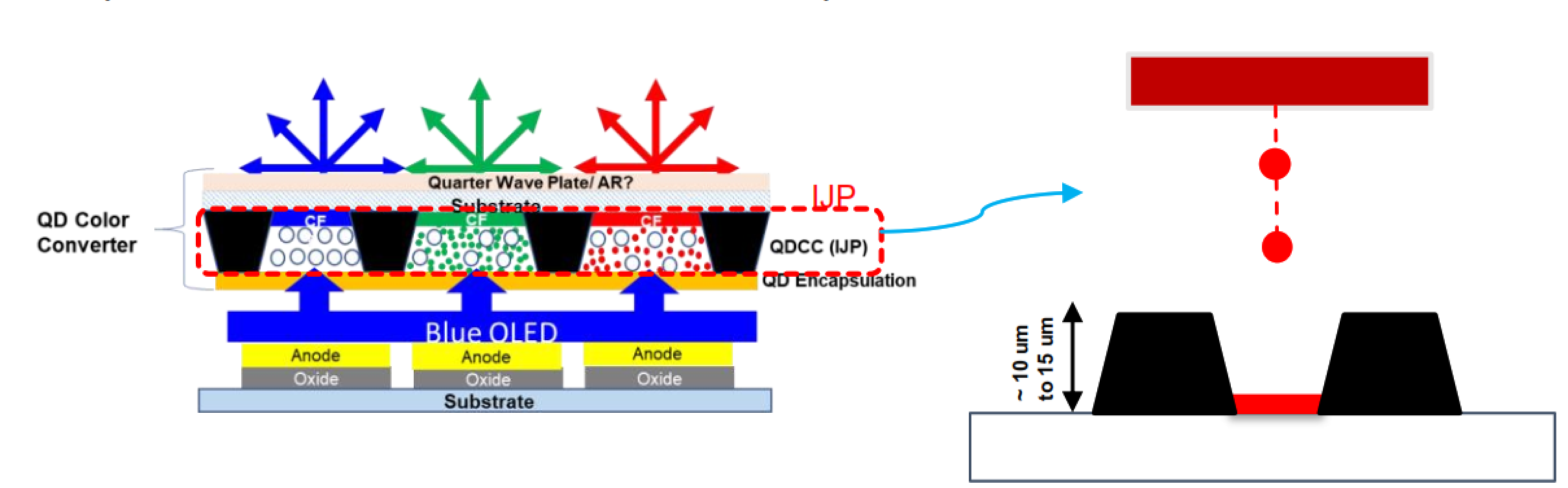 Printing of QDs for QD-OLED (Credit: Sid Mohan, DSCC at SID Display Week 2020) Click for higher resolution
Nanosys was omni-present as always, this year with some important press releases, and creative marketing with a “giving back” BT2020 mural, “movie night” with color analysis, and daily interviews on “The Display Week Show” with important leaders in the field. My personal favorite was the interview with Dr. Paul Alivisatos of UC Berkley. For those of you who don’t know him, he is a figurehead in the field of quantum dots and his excitement is contagious when it comes to nanotechnology. Notably, he was the co-recipient of 2020 Jan Rajchman Prize alongside Moungi Bawendi (MIT). Their combined research laid the groundwork for the QLED displays we see today.
 The mural in Oakland, CA painted by artist Chris Granillo as part of Nanosys’ “giving back” campaign (Credit: Nanosys at SID Display Week 2020) Click for higher resolution
Nanosys announced three important business updates at SID and in the days following.
First, they announced an exclusive distribution agreement with Nagase to expand their reach around the world. Additionally, they announced a materials supply agreement with Shoei Chemical (Japan). This is a key upgrade to the QD supply chain for those relying on Nanosys for materials, especially for customers in Asia. I suspect this is, in part, a response to Nanosys needing to shut down for 2 months during the peak of the pandemic here in the US while Asia was starting to reopen factories. Having QD production duplicated in Asia will reduce risk and lower tariffs for many customers.
Finally, Nanosys announced a Series I (that is the letter i, not numeral 1) investment in the amount of $20M from Shoei Chemical to bring their total investment to ~$186M (source: Crunchbase). I hope their valuation/exit strategy supports this sort of investment!
GE Matching QDs in Red
GE’s Jim Murphy took us through some recent technological advancements in their KSF/PFS narrow-band red phosphor (Bob covered this last week), which is widely present in every major display category (mobile, tablet, monitor, lap top, TV). It’s no secret that this high-performing phosphor has been a challenge for QDs to compete with in terms of simple implementation for LCD, and GE showed that it can match or beat most QD materials in terms of red color point too. One area where we (QD enthusiasts) have always been able to claim an advantage is in size (nm vs microns). GE has apparently been working hard on this problem as they shared a video of KSF being ink-jet printed on a substrate to form a glowing red GE logo. No word on the exact size or performance, but they did say it was “sub-micron.” It is important progress as the smaller sized phosphors will also be necessary for mini-LEDs which are becoming a highly sought after technology for local dimming HDR displays.
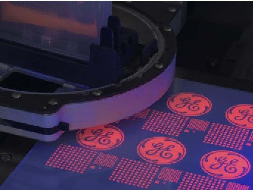 GE’s KSF phosphor (sub-micron sized) being printed via IJP (Credit: Jim Murphy, GE, SID Display Week 2020)
It’s worth noting that KSF is now making a push to multiple form factors to satisfy consumers in multiple display markets. The typical use-case for KSF in LCDs is mixed with a green phosphor on chip over a blue LED. While this package is still common, they also are pursuing “magenta” LEDs with only KSF on blue LED (possibly for use with a green QD film like perovskite), as well as a down-converting film that contains KSF, acting like the QD films we see in use today. GE has also been working on a narrow band green phosphor (not as narrow as KSF) which they are currently sampling to customers.
Be on the lookout for SID Display Week 2020: QD Review Part 2 where I will dive into the technical symposium and walk the virtual show floor. Thanks as always for reading!
Peter Palomaki is the owner and chief scientist at Palomaki Consulting, a firm specializing in helping companies solve big problems at the nanoscale. His utilizes his expertise in quantum dots and materials chemistry to solve challenging problems with clients large and small.