I wanted to write about an event that I look forward to every year, the QD Forum. Unfortunately, given the current pandemic, the event had to be postponed. When the QD Forum does happen, you can bet I’ll be there to report on it! In the meantime, I offer you some thoughts on a technology that has had real impact in the display world recently. QD-OLED.

Perhaps some of you heard the news about Kateeva laying off nearly 150 people earlier this year? Well there is a direct link between this layoff and Samsung’s QD-OLED plans. It seems Kateeva got the short end of the stick as Samsung has chosen Semes to provide ink-jet printing equipment for the QD-OLED project on the Q1 line. Kateeva was banking on this customer to expand their IJP equipment into a new product line, so the blow was a big one for the relatively small company.
Now Kateeva will focus on their core business of IJP for thin film encapsulation (TFE), a business they have done quite well in for the past few years as mobile OLED displays continue to be the go-to choice and gain market share. This means, however, that all QD work at Kateeva will cease immediately. There was a heartfelt summary statement on their website from the CEO, but it has since been removed.
Presumably the IJP equipment from Semes will be used to deposit the QD color-converter layer above the all-blue OLED sub-pixels. To battle the poor blue OLED lifetime, it seems Samsung will use a triple stack of blue OLEDs which will reduce the stress on each individual emitter layer resulting in longer lifetime. Even if the OLED does degrade over time, if all the sub-pixels degrade at the same rate then there will be no color point shift, only a slow decrease in brightness… in theory.
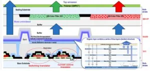
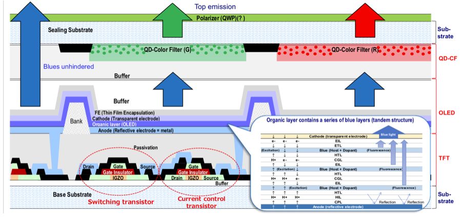 One of the more detailed graphics of QD-OLED I could find. Source: OLED Association
As I have stated before, the requirements for the QD layer in this device are much different than on the current implementation architecture of QD film. In QD-OLED the QDs must be highly concentrated to absorb as much blue light as possible. The QD layers must be highly uniform in thickness as this will directly impact the brightness of each sub-pixel, in turn impacting uniformity. One benefit (to the QDs) is that the QD layer is at the front of the screen so the intensity of blue light is probably far less than what is seen in the backlight unit where QD films sit. Additionally, the QD layers will likely be deposited on a glass substrate (see figure above) so encapsulation is inherent on one side. This means encapsulation (using TFE perhaps) is only required on one side of the QD layer. Implementation of QD films requires a barrier film on both sides of the QD layer.
So why did Samsung choose Semes over Kateeva? For starters, Semes is mostly owned by Samsung, so it keeps the technology close to home. Additionally, Semes is a larger company and has a suite of display equipment available, so if Samsung chooses Semes for other tools there may be some benefit in both price and continuity. Even though Samsung relies on Kateeva for TFE of OLED displays it seems Kateeva will not be participating in the QD-OLED game anytime soon.
So what will QD-OLED look like? There was a small demo at SID Display Week 2019 by CSOT, but to be honest it did not impress anyone. It was reported that Samsung showed a QD-OLED at CES earlier this year, but behind closed doors. In theory QD-OLED displays should have all the benefits of OLED (viewing angle, deep blacks, thin form factor) along with the color purity and efficiency that QDs bring to the table. If SID Display Week is not cancelled in 2020 I’m hopeful we may see a QD-OLED display there. But given these uncertain times it seems more likely we’ll get our first real glimpse in 2021.
The announcement of Kateeva layoffs reminds me of QD Vision in 2016 which signalled the beginning of the end. I hope the same isn’t true for Kateeva. Best of luck to all those impacted, especially during these uncertain times.
Peter Palomaki is the owner and chief scientist at Palomaki Consulting, a firm specializing in helping companies solve big problems at the nanoscale. His utilizes his expertise in quantum dots and materials chemistry to solve challenging problems with clients large and small.