
Scrona, a startup spun out of ETH Zurich, is developing a novel printing technology called electrohydrodynamic (EHD) printing. Scrona aims to replace photolithography for certain manufacturing processes in semiconductors and advanced packaging. EHD printing’s combination of precision, scalability, and low-cost fabrication of micro- and nano-scale structures makes it well-suited for advanced flexible electronics. With further development to expand material options and improve manufacturing throughput, EHD printing could enable mass production of stretchable LED displays, electronic skins, biosensors, and other emerging technologies.
Avantama specializes in creating high-performance quantum dot (QD) inks, specifically perovskite QDs. The optical and electronic properties of QD are highly dependent on their size. This size-dependency allows for precise control over the color and brightness of the light they emit, which is why they are valuable in display technology. Perovskite QDs have high absorption coefficients. This means they are very effective at absorbing light. In display technology, this efficiency can lead to more vibrant, bright, and color-rich displays. are defect-tolerant. This is an important characteristic because it implies that these QDs can maintain high emission efficiency without the need for an additional passivating shell, which is often required in other types of QDs to prevent energy loss. This defect tolerance contributes to the high performance of the perovskite QDs.
Scrona and Avantama have just revealed they have effectively processed high-performance quantum dot (QD) ink through Scrona’s EHD inkjet printing, merging the inkjet technology’s advantages with superior patterning resolution to develop MicroLED displays. Scrona :
- Efficiency and Tact Time: Production of MicroLED displays becomes more efficient and faster.
- Reduced Printhead Nozzle Count: A significant reduction in the number of nozzles needed in the printhead, by a factor of five.
- Thinner Pixels with High Optical Density: The ability to print thinner pixels that still maintain high optical density.
- Waste-Free Process: The EHD process is described as additive and waste-free, which could mean it’s more environmentally friendly and cost-effective.

I talked to Walter Braun, COO of Scrona, regarding the company’s novel EHD technology. Braun outlined Scrona’s unique printing method in which they integrate EHD nozzles into microelectromechanical systems (MEMS). As he explained, “We apply an electrical field from the outside of the nozzle. And by doing this we generate a meniscus of fluid material, and if we tune the electrodes and the voltages right we focus all the energy to the tip of that meniscus and only from there we release droplets.”

This technique allows Scrona to overcome limitations of standard inkjet printing and achieve much higher resolution while still being able to scale to high nozzle density. Braun set the goal to reach “printheads in the future, with the same nozzle count as incumbent inkjet printers, like 1,000 or 2,000 nozzles.”
When asked about key advantages versus inkjet, Braun emphasized two main benefits:
- Printing feature sizes under 500 nm, over 10x smaller than inkjet
- Ability to print thick fluids loaded with functional materials rather than just thin liquids
Braun sees equipment manufacturers in the semiconductor and PCB industries as Scrona’s primary customers. He shared examples such as replacing numerous photolithography steps for redistribution layers in advanced packaging.
Braun explained that EHD printing has superior precision, materials compatibility, and cost-effectiveness. It can print detailed patterns directly onto flat or curved surfaces using functional inks made from materials like quantum dots, nanowires, graphene, polymers, and metal nanoparticles.
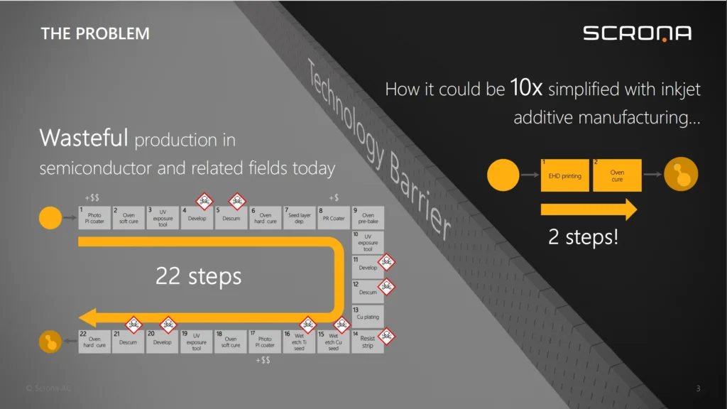
Braun recounted a recent conversation that highlighted the issues faced by display manufacturers in a similar vein: “They said well it’s not sustainable, because with the incumbent process we follow the topography, they waste about 90% or 95% of the material.”
EHD Printing and Displays
EHD printing is, by some accounts, emerging as a revolutionary technology in the field of display manufacturing, particularly for the fabrication of high-resolution quantum dot LED and MicroLED displays. It’s safe to say that in theory it does address the limitations of traditional piezoelectric inkjet printing, which struggles to produce sufficiently small pixel sizes for high-definition displays. So, EHD printing’s ability to create its ultra-fine patterns makes it ideal for developing high-resolution displays like those required for mobile and wearable devices. Obviously, Scrona has to still scale its processes up, but scaling is achievable and on the horizon.
EHD also seems to allow for fine control over the line width of printed material by adjusting the ink viscosity and printing speed. The ability to control various parameters like pixel size, ink viscosity, and printing speed offers vast flexibility in designing displays with specific characteristics. In addition, EHD printing facilitates the fabrication of both top and bottom-emitting quantum dot LED devices. The top-emitting devices, in particular, offer advantages like higher aperture ratios and efficient light out-coupling, making them suitable for mobile and AR/VR displays. Compared to traditional methods like fine metal mask (FMM) patterning, EHD printing should be more cost-effective and efficient, making it a promising technology for mass production. The future looks bright for EHD printed displays and Scrona is a company to watch.