A team of researchers, led by Professor Ji-woong Yang from DGIST’s Department of Energy Science and Engineering, has been developing a novel double-layer dry transfer printing method. This innovative technique, created in collaboration with Professor Moon-kee Choi from UNIST’s Department of New Materials and Dr. Taeg-hwan Hyun of the IBS Nanoparticle Research Center, aims to create a new approach to high resolution displays the field of augmented reality (AR), virtual reality (VR), and wearable displays by enhancing their efficiency and resolution.
Quantum dot (QD) nanoparticles have emerged as the next-generation materials for display technology due to their remarkable properties, including high color purity and excellent color reproduction. Despite these advantages, the traditional method of dry transfer printing—where QD ink is applied to a substrate—has struggled to achieve widespread use in display production. This is largely due to its low luminescence efficiency, typically falling below 5%, which hampers its practical application.
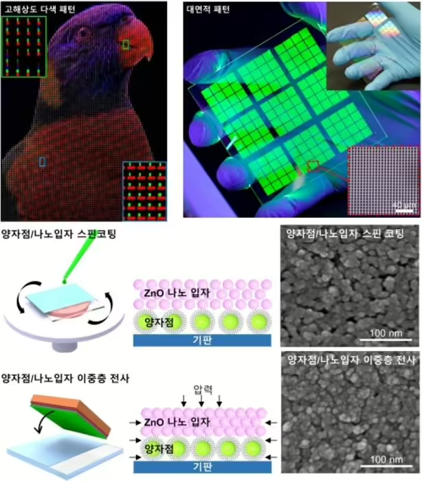
In response to this challenge, the research team has developed an advanced dry transfer printing technology that simultaneously transfers both light-emitting and electron-transferring layers onto a substrate. This method significantly reduces interfacial resistance, a key factor that hinders electron injection and contributes to charge leakage during device fabrication. By addressing these issues, the team was able to enhance the external quantum efficiency (EQE) of the QLED devices to an impressive 23.3%. This level of efficiency is remarkably close to the maximum theoretical efficiency of quantum dot light-emitting devices, marking a significant achievement in the field.
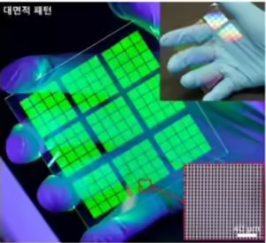
The new double-layer thin films created through this technique are not only highly efficient but also enable ultrahigh-definition patterning. The researchers successfully produced RGB pixelated patterns with a density of 2,565 pixels per inch (PPI) and monochromatic QD patterns with an extraordinary density of up to 25,526 PPI. Furthermore, they demonstrated the scalability of this technique by printing an 8 cm x 8 cm area, confirming its potential for mass production and commercialization.
Professor Ji-woong Yang emphasized the significance of this development, noting that the devices fabricated using this technology exhibited an EQE of up to 23.3%, a result that closely aligns with the theoretical maximum for quantum dot light-emitting devices. Similarly, Professor Moon-kee Choi highlighted the potential of this technology to enhance resolution in VR and AR displays, with further research aimed at broadening the application of quantum dots to smart wearable devices.
Reference
Yoo, J., Lee, K., Yang, U.J. et al. Highly efficient printed quantum dot light-emitting diodes through ultrahigh-definition double-layer transfer printing. Nat. Photon. (2024). https://doi.org/10.1038/s41566-024-01496-x