Chances are you missed the Recent SID Webinar on display backplane evolution given by SID Fellow Dr. John Wager, professor at the school of EECS, Oregon State University. Wager said important to the evolution of the display backplane is not only “electron mobility and transport” in addressing ever more pixel dense panels, but “process complexity” which plays a critical role in the future of backplane development.
![]()
Most attending any kind of seminar on this topic of backplane development will have heard of the importance of the electron mobility in supporting the trends toward ever higher density displays. But Wager also made the case for reducing the manufacturing process flow leading to lower cost in this profit margin squeezed industry. In his February 17th talk given at OSU for the Pacific Northwest Chapter of SID he took the audience through the past, present and (at least one) future backplane technology alternative looking at process complexity.
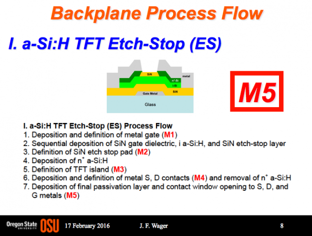
On the traditional amorphous Silicon (a-Si) process side, Wager identified five key steps to the TFT Etch-Stop (ES) manufacturing method. Improvements in the a-Si process came with a Back-Channel Etch (or BCE) approach which reduced the process to four steps (see slides.)
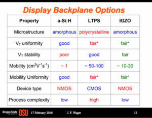
Wager noted that the trend in high pixel dense small displays brought about the need to move beyond traditional amorphous silicon toward the polycrystalline backplane offered by LTPS (low temperature polysilicon) with its excellent electron mobility characteristics (see chart).
LTPS backplanes continue to serve the small display market well, including AMOLEDs. But the attempt to scale the LTPS solution to ever larger displays with mother glass reaching multi-meter sizes met with real process problems, adding to both complexity and cost of panel manufacturing.
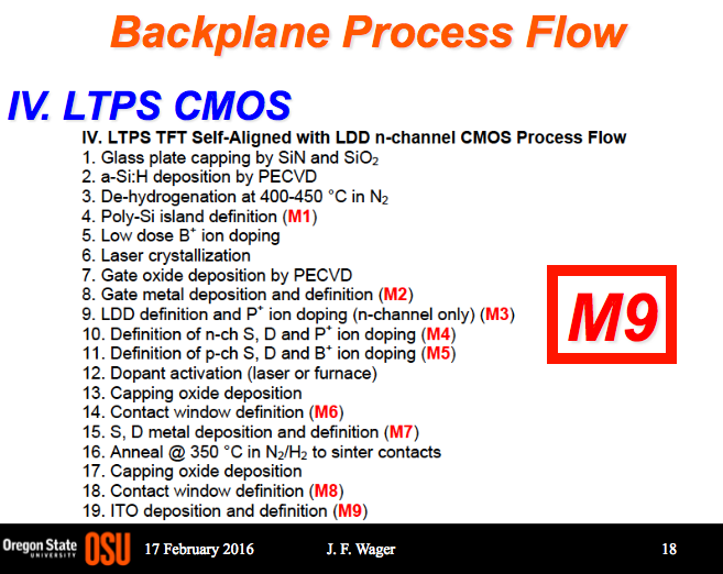
And while the backplane process flow for LTPS nMOS type was at parity with a-Si at four major processing steps, moving to an LTPS CMOS solution would balloon the processing to nine steps, adding complexity and cost. Scaling up LTPS for large size displays, just doesn’t seem to be an option.
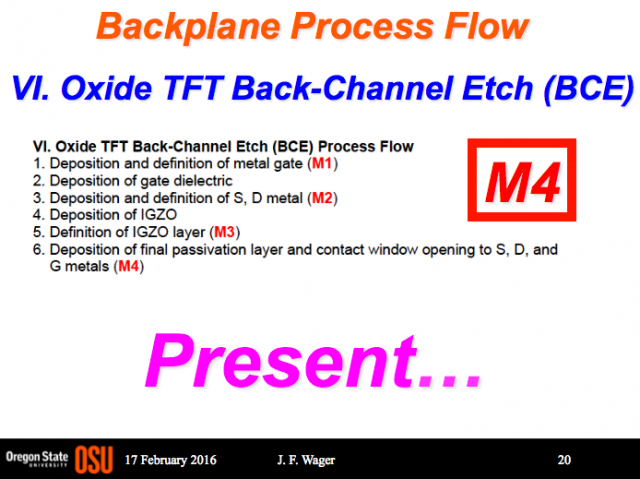
 Enter Oxide TFTs (IGZO) displays that offer suitable electron transport properties to address large displays, plus scalability and many fewer process steps when compared to LTPS. Here current process steps are down to four, using a BCE approach, and the future holds the potential for even higher efficiencies as research work and private corporate development continues. You can find an expanded look at this in Wager’s recent editorial:Amorphous? Again? found in Information Display Magazine on the SID.org web site.
On the production side, Wager noted that today Sharp, Samsung and LG are all shipping displays using Oxide TFT backplanes (with Sharp and LG doing this in Gen 8 fabs). Production volume from these three manufacturers is over 100K sheets per month according to Wager’s reckoning with another 280K/month planned to be added this year by the group. On top of this, BOE, CPT and CEC Panda all have announced plans to move to Oxide TFT manufacturing in 2016. Current shipping products using Oxide TFT backplanes range in display size from 4.7″ to the 76.7″ curved OLED TV from LG.
“Retina-Class” displays were made popular by Apple, offering pixel density beyond human visual acuity in early versions of its iPhone and iPad products. This came with a healthy competitive push from market leader Samsung which offered high density AMOLED displays and which has established a track record of performance excellence with each successive iteration of its Galaxy S series products.
The trend continues with large displays moving from FHD (full HD 1920 x 1080 pixel) to the now (almost) standard 4K or UHD displays with 3840 x 2160 pixels (or 8.29 megapixels), and most certainly progressing toward 8K with its whopping 7680 x 4320 pixel density (or 33.18 megapixels).
What the future holds for IGZO technology, it will most certainly have to accommodate the growing share of pixel dense displays as the market continues its, seemingly insatiable, appetite for pixels and display real estate. But to get there will require not just the right materials like IGZO or some future exotic chemical formulation, but the process efficiency and know-how to bring the technology to market. – Steve Sechrist