We published an article on Porotech’s technology, which could be important for microLED at the end of last year. Now the firm has some more investment and we caught up with CEO Tongtong Zhu to find out more.
 Here’s a (very) brief introduction to the technology. Most LEDs are based on GaN technology, but the most efficient colour by a long way is blue. Green and Red are not made using GaN in individual LEDs. You could make microLEDs using the different architectures but that gets very complicated in manufacturing as well as making driving more complex. The other problem is that red LEDs get much less efficient when the edge size of the LED gets down to below 10 microns.
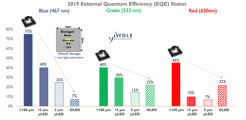 All microLEDs using regular LED technology get less efficient as they get smaller, but its worst for Red. Source:Yole via OLED A
You might think that 10 microns is pretty small, but for many of the applications where microLED might be used, the sizes have to be that small to make the economics work. If the LEDs are bigger than that, each one costs too much. Remember, there are 24 million microLEDs needed for an UltraHD/4K display. Or, to put it another way, every 40 displays is another billion LEDs!
So one approach is to use blue GaN LEDs and then perform colour conversion for the red and green. However, if you want to use QDs, and you might want to in order to get as close as you can to Rec. 2020, that’s a challenge as QDs, so far, do not like to be deposited on the LED because the heat affects the QDs. (Having said that, Nanosys has bought Gl?, so it thinks it has a solution to that).
The other approach is to somehow make red, green and blue using GaN technology. That’s what companies that we have reported on like Aledia, Gl?, Plessey and Soitec have been working on. The first two have been working on nanowire approaches so that the LEDs can be made on silicon but needs new semiconductor techniques. Nanosys’ CEO, Jason Hartlove, has said, after buying the Swedish company, that Gl? has great epi technology, but Zhu pointed out that nobody is actually making the devices in volume yet and it can be really hard to get semiconductor makers to adopt new technologies. That comment reminded me of LCD makers – it can be very hard to get them to change their pixel designs. That has been the downfall of a number of potentially disruptive technologies that I have reported on over the years.
No Change for LED Makers
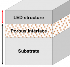
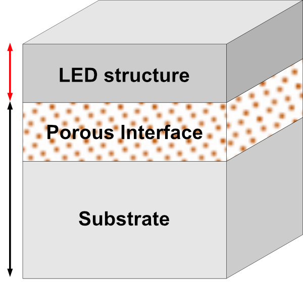
On the other hand, Zhu told us that the fundamental difference in the Porotech approach is that it doesn’t involve any change to traditional LED making techniques, although there is an extra step that Porotech performs. Art described the technology in December (Porotech Offers Native Red LED Epiwafers for MicroLED Applications), but basically it exploits channel dislocations in the wafer and an etching process is performed to get etchant to flow into the material to make ‘nanopores’. The LEDs can be made on silicon or sapphire platforms as it works on the InGaN layer, not the underlying substrate.
After the LED maker has designed and grown the epi layer on the substrate. The wafer is sent to Porotech which creates the porous layer in the epi material and returns the wafer to the LED maker to grow the LED device on top using normal MOCVD processes.
Zhu told us that the ‘standard recipe’ for making green LEDs turns out red LEDs after production using the processed InGaN wafer.
In its press release, Porotech said that it is first targeting microdisplay application, that is to say not individual microLEDs but monolithic displays. That’s a fairly obvious application if you have a technology that can work when based on silicon-based LEDs. Head-up displays will be a key early market for microLED-based systems as the high brightness is a big advantage, and a necessity for good AR which has to compete with high ambient light. Of course, monolithic microdisplays do not depend on the kind of mass transfer process which still need to be fully developed and industrialised.
Microdisplays are also a good market for ‘smart pixels’ which is to say, display devices that sit on top of a standard CMOS IC substrate so that circuits to control the pixel are integrated. Smart pixels are a target for Porotech.
Part of the £3 million ($4.15 million) investment at Porotech is to boost its capacity to process wafers in Cambridge. At the moment, Zhu told us, it can process around 120 wafers/week (6″ equivalent) but it is scaling up to work better with larger CMOS wafers. There is no fundamental reason for a limit on substrate size.
I’ve used the phrase “If they can do what they say they can do…”. This writer is not qualified to know if they can do what they say and typically this kind of radical development often has a ‘gotcha’ somewhere, but in the case of Porotch, if what is claimed is true it could be significantly disruptive to other microLED companies. Clearly, the firm’s investors are convinced as this round of investors includes four previous investors.
The technology is not just confined to applications in the display field, but this writer is! (BR)