Last week, I (Bob the editor) wrote a Display Daily on metasurfaces and the ways that new techniques are being used to bring new and quite dramatic changes to optics – and which may have a big impact on the development of AR/VR and projection displays. (Is There Really “No Moore’s Law for Optics”?) The article provoked more response than usual – perhaps we should change to Optics Daily!

One of those that contacted me was Ken Li, well known in the display industry, and a previous regular contributor to Display Daily (I referred to one of his articles in my one last week) and he wrote an extended article as follows:
“After reading your article on “Is There Really “No Moore’s Law for Optics“?” and my old article on “My Etendue Story” from the link, I couldn’t help sharing my thoughts as written below regarding traditional optics and metasurface optics.
I started to think about sub-wavelength structures many years ago as I was working with the high output LED from Luminus which had a photonic lattice. I was trying to come up with a simple-to-visualize model of such structure. I imagined myself to be a photon going through the photonic lattice. I could not see anything as my wavelength was longer than the features of the photonic lattice. On the other hand, I could feel the difference entering the photonic lattice from the LED semiconductor layers. As a result, I told myself that I could feel the “mixed” solid materials and the air in between, which I could not “see”, but I responded to it by moving faster or slower. Hah, that’s the change in refractive index!
As a “wave”, I would have a hard time visualizing this. But as a photon, I can “feel” the difference. Please bear with me on the use of the terms “see”, “feel”, “visualize”, etc. It does not seem to have a good rule or definition in using them. In this context, they could not be defined easily, but have to be “realized”. I hope you do realize what I’m trying to say.
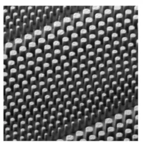
I looked at the metasurface optics picture from the article as shown above, I started to think about the structures. Traditional optical elements are something we can touch and feel as macroscopic structures. However, the metasurface optics are too small to be touched and felt, and as a matter of fact, they are too small to be seen, but we can see and feel the effects of such metasurface optics.
I was looking to pave a small section of my backyard so that I can walk on them and not get dirty, but not using concrete. I was considering using some small gravel stones or pebbles. The gravel or pebbles have to be small enough so that I do not feel the individual pieces when I walk on them. The exact sizes would not be important, but I know that I would feel differently based on the sizes of the gravels or pebbles used. I came across the picture as shown above as I was searching through the web. This shows a small section of paving material with varying sizes of pebbles and spread unevenly. I thought that if the paved path has the same unevenness, I will have a changing feeling on my feet as I walk on along the path. After looking at this, I immediately thought about the metasurface optics shown in the article, showing sub-wavelength features with varying dimensions. I started to ask what the photons would feel.
Coming back to the fact that “it still seems to be true that “there’s no Moore’s Law for optics”, it may be more accurate to now say that “optics can really benefit from the technology developed to support Moore’s Law””, I think this is an illuminating conclusion at any wavelength. As microelectronics becomes nanoelectronics, and further into pico-electronics, the gravel and pebbles as described above become sand in which there will be no limit to the creation of new structures and could only be limited by one’s imaginations. I could not imagine when femto-electronics is reached. By that time, all the sand will become dust and it will be everywhere and hopefully be under control. At this time, I am happy staying with the 5 nm technology making the M1 chip possible for my new MacBook Air”. (KL)
Another reader also contacted me to highlight that
“Part of the problem is that the traditional fabrication techniques for curved optics (grind, polish, interferometric testing), even in their most advanced versions (like deterministic magnetorheological) are slow and subtractive.
The additive approach by Luxexcel sounds really impressive, beyond just eyeglasses. As does this…”
I had to look up deterministic magnetorheological polishing – interesting, but the two additive optical element creation systems that use inkjet printing to create components that don’t need polishing. I have been keeping half an eye on 3D printing for a long time, but I hadn’t thought much before of the potential in optics. (although we did spot an article in our WBS service that Luxexcel had done a deal for equipment to make its optics in September. (BR)


