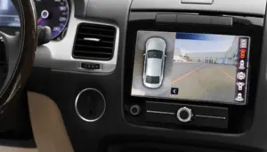
Omnivision has been peeling back the curtain on its OX08D10 8-megapixel CMOS image sensor with TheiaCel technology at AutoSens Brussels. It’s supposed to bolster automotive safety by enhancing resolution and image quality in exterior cameras for advanced driver assistance systems (ADAS) and autonomous driving (AD). In the automotive realm, LED traffic light flicker has long posed challenges for imaging, often hindering ADAS and AD systems from accurately discerning illuminated traffic signs. HDR, and high resolution are now indispensable in contemporary automotive image sensors to push towards higher autonomy vehicles. This is also good news for the display industry because it makes a case for brighter, higher resolution, better displays in cars.
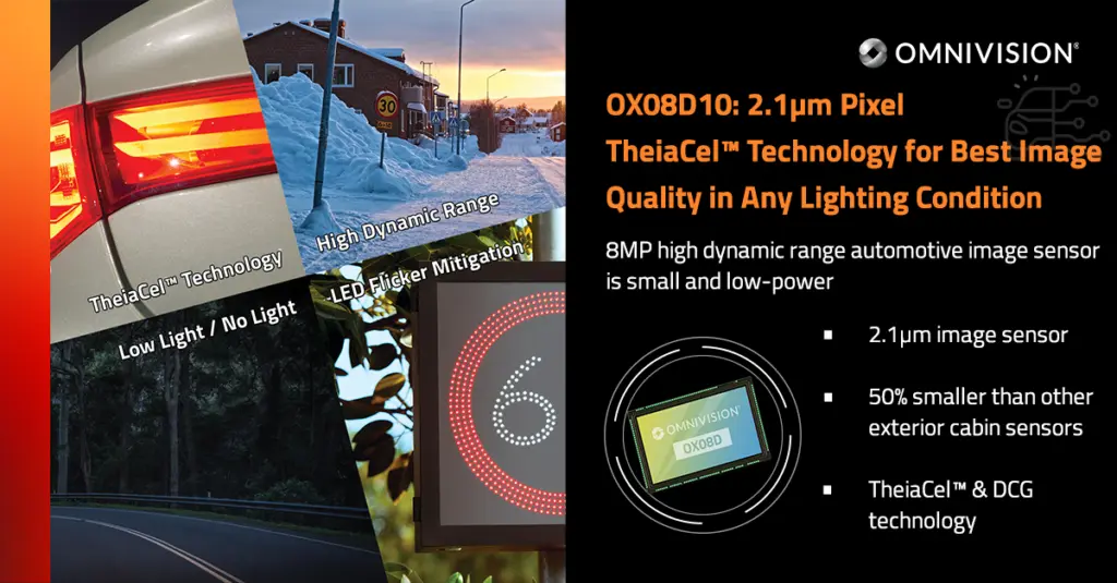
The OX08D10 is being promoted on the basis of its lowlight performance, low power consumption, and a compact size that is 50% smaller than other exterior cabin sensors in its class. It is the first image sensor to integrate Omnivision’s new 2.1-micron TheiaCel technology. This is technology that leverages the power of next-generation lateral overflow integration capacitors (LOFIC) and Omnivision’s DCG high dynamic range (HDR) technology, negating the effects of LED flicker regardless of lighting conditions. TheiaCel allows the OX08D10 to achieve an HDR image capture range of up to 200 meters, optimal for automotive exterior camera applications.
Omnivision claims that in a head-to-head with its non-LOFIC-based precursor, the OX08D10 emerges superior in several metrics. Specifically, its LED flicker mitigation (LFM) dynamic range is 3.3x higher, and the total dynamic range is nearly three times greater. The sensor also integrates enhanced cybersecurity measures in line with the latest MIPI CSE version 2.0 standards, incorporating functional safety to automotive image sensor data streams. It also has a chip scale package (CSP) package technology. This is a type of integrated circuit package that has a size very close to the actual semiconductor die size. The benefits of CSP include a smaller footprint for the device, potential cost reductions, and improved performance due to shorter interconnects. As of now, samples are available for review, with mass production slated for the latter half of 2024.