It is desirable to make micro LEDs as small as possible. One potential benefit of doing so is to enable more compact microdisplay based display devices. The good news is that conventional blue and green micro LED chips can and have been successfully reduced in size. It has, however, proven difficult to reduce the size of red micro LED chips to less than 50 ?m.

A recent development on addressing the red micro LED issue comes from Nitride Semiconductors Co., LTD (Tokushima, Japan). The company has reported progress using an approach for producing red (as well as green and blue) light emitting micro LEDs that is based on the use of an ultraviolet emitting microLED to excite various phosphors. More specifically, the company has developed means to minimize factors that limit the emission of ultraviolet light from UV LEDs.
First a few words of background information.
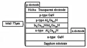
Epiwafers for ultraviolet emitting LEDs are typically fabricated utilizing the epitaxial growth of LED structures on sapphire substrates by means of metal organic chemical vapor deposition. A cross sectional diagram of a typical LED chip structure is illustrated in the figure below.
 A cross sectional diagram of a typical LED chip structure.
The InGaN layer is key to a LED that emits blue light. Variations made to the composition of the indium enables adjustment of the wavelength of the emitted light all the way from the infrared through to the ultraviolet. It turns out, however, that the luminous efficiency of LEDs maximizes in the wavelength range from 400 to 420 nm. It has been further found that the luminous efficiency of ultraviolet emitting LEDs decreases rapidly at wavelengths shorter than 380 nm.
There are two principle reasons for the decrease in the efficiency in emission of ultraviolet light. The first is that, as the wavelength decreases, there is a “deterioration in the non-uniformity in the InGaN layer” and this causes “a reduction of transforming density.” The second is increased absorption of the emitted light at wavelengths lower than 370 nm caused by dislocations in the GaN layer. It therefore follows that, to improve the efficiency of light emission at shorter wavelengths, it is necessary to increase the non-uniformity and to reduce the dislocation density in the activated layer.
To achieve these goals, the first step used by Nitride Semi derives from the observation that GaN has a bandgap is 3.4 eV (producing an emission at 365 nm). To achieve production of a shorter wavelength of light, the company employed a “four-mixed crystal of AlInGaN using AlN” which has a bandgap of 6.2 eV (producing an emission at 200 nm).
Increasing the non-uniformity in the composition of the light emitting layer was accomplished by inserting a region of nanosized Ga droplets. In addition, a discrete layer of SiN was added to vary the diffusion length of the composition and increase variation in band gap. These changes served to double the ultraviolet light emitting efficiency of AlInGaN.
Next, a method was developed to reduce the density of crystalline dislocations. This was accomplished by the use of a high temperature SiN intermediate layer, a low temperature GaNP buffer layer and a low temperature SiN buffer layer.
Collectively, using these techniques, Nitride Semi was able to accomplish the following:
- The chip size of a conventional ultraviolet emitting micro LED is 16 ?m x 48 ?m. The chip spacing is 10 ?m in the horizontal direction and 30 ?m in the vertical direction. Given these dimensions, about 3.4 million chips can be fabricated on a 4 inch wafer.
- The newly developed ultraviolet emitting micro LED chip has a chip size of 12 ?m x 24 ?m with a chip spacing of 5 ?m in both the vertical and horizontal directions. Given these dimensions, about 14 million chips can be fabricated on a 4 inch wafer.
The increase by a factor of about four in chips per wafer can reduce the cost per chip using the new technology to one fourth that of an equivalent chip fabricated on a conventional wafer. More generally, the company claims that, with these means, higher productivity is possible without additional complication in the processing of the wafers. Finally and most importantly, the researchers report good electrical characteristics for chips fabricated using the new technology.
At this time, the company is developing methods for mass producing chips using the new technology. Nitride Semi has stated that the company has licensed the new technology to a LED manufacturer. – Arthur Berman