Electronic displays are fundamentally devices for converting electrons to photons. The more efficient you can make them in this conversion process, the brighter they are for the same power or the lower power they use for a particular brightness. There are two key numbers when checking the efficiency of a device, the IQE and the EQE, the internal and external quantum efficiency factors.
The IQE is interesting because it shows how optimised the device is as a display. If all the electrons are converted, you know that the light production cannot be improved. However, it’s EQE that really matters. The EQE shows how much of the light that you have created can actually get out of the device in the direction you want.
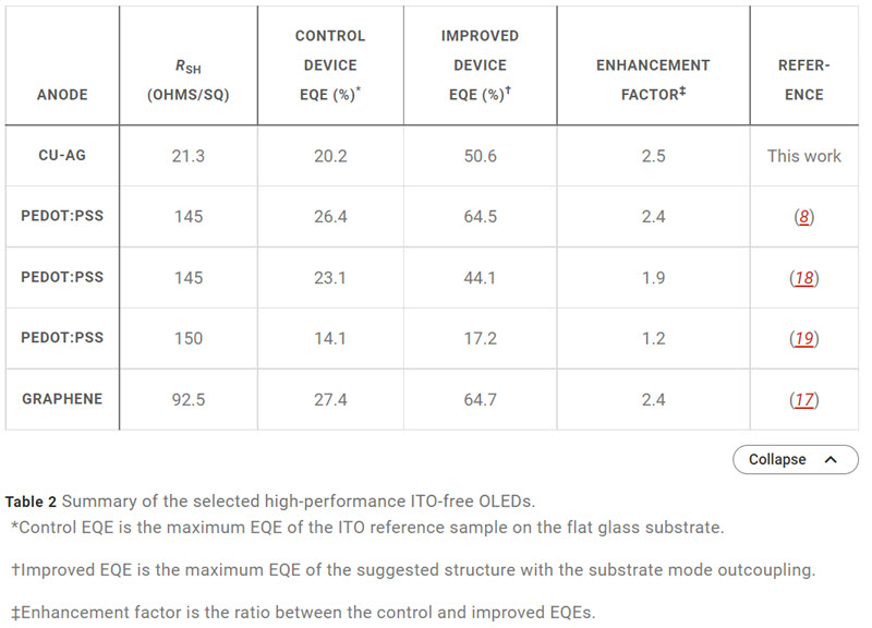
The good news is that red and green OLEDs, using phosphorescent and TADF OLED materials, can get to 100% IQE. That’s fantastic for great battery life and high brightness. However, there’s bad news as well. The EQE of OLEDs drops to around 20%. That is to say that without some technology, only 20% of the light generated actually makes its way out of the device. We’ve been reporting on this topic for a number of years with companies such as Pixelligent who have designed materials that help with this problem.
One of the key challenges in getting light out of the OLED is Total Internal Reflection (TIR) – the phenomenon that is exploited in optical fibres. Light can be trapped inside transparent substrates, bouncing between the surfaces of the different materials that are around the layer containing the light.
There are three areas that cause light to be lost and a group at the University of Michigan have focused on one of these, the losses caused by the light in the OLED stack trapped by the OLED stack and the transparent conducting electrode on the top of the device. In their paper, the group details different approaches to solving the problem by replacing the ITO that was the first material used for electrodes, but these use carbon-based materials, such as graphene, conductive polymers, and optimised PEDOT:PSS/Titanium Oxide and graphene. However, all of these solutions involve significant and difficult processing.
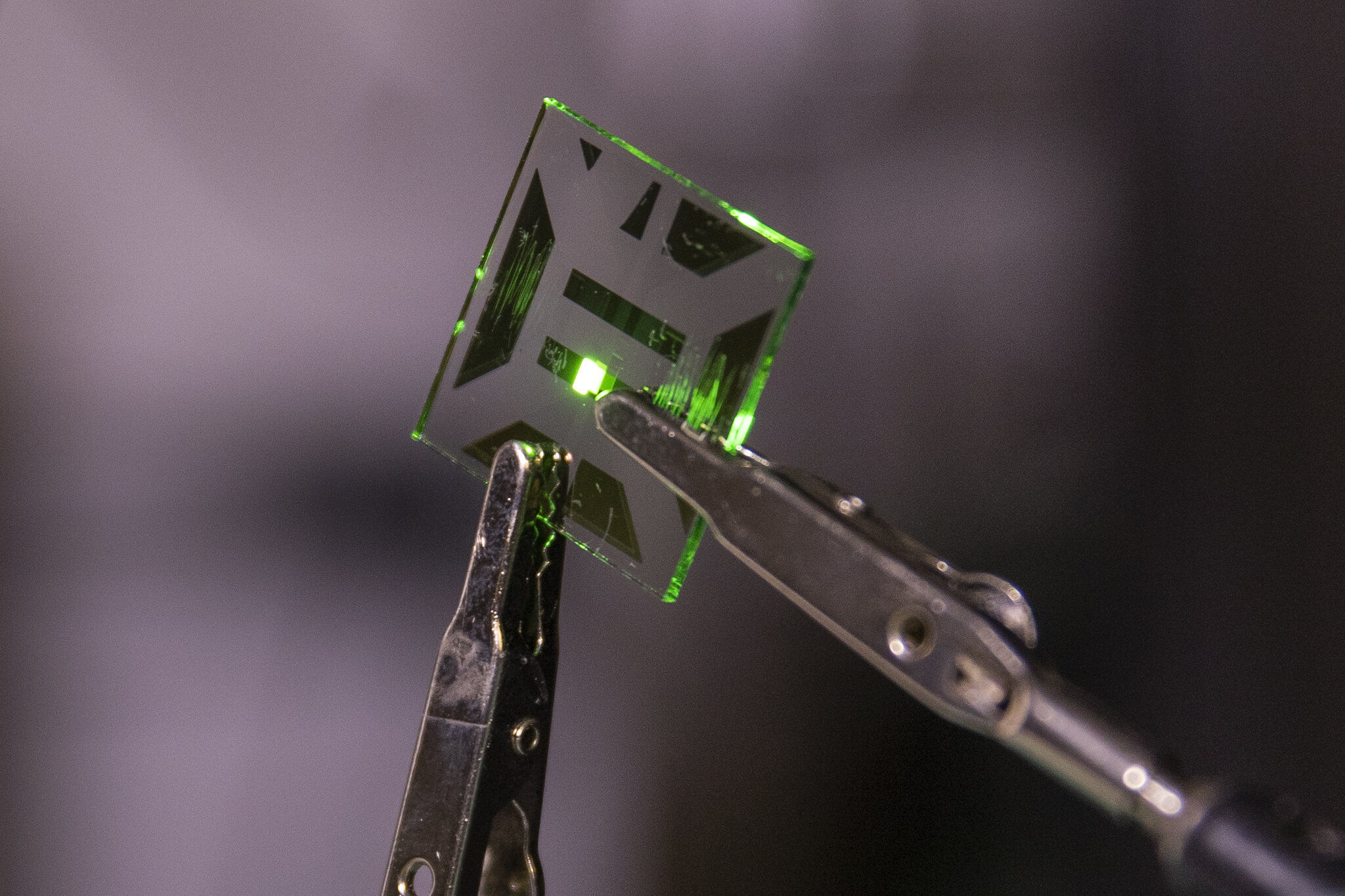
Research showed that by replacing the ITO layer with two very thin layers – 5 nanometres of silver on top of a copper seed layer – the waveguide loss is eliminated completely. The key is that these layers can be deposited using the same vacuum chambers that are already used in OLED manufacture to deposit other layers, so it is relatively simple to introduce in industrial production.
“Industry may be able to liberate more than 40% of the light, in part by trading the conventional indium tin oxide electrodes for our nanoscale layer of transparent silver,”
said Changyeong Jeong, first author and a Ph.D. candidate in electrical and computer engineering.
The paper describes a bottom-emitting OLED that it made for testing, but the material can also be used for top-emission OLEDS (as discussed by Barry in his DD yesterday (The Flat Panel Industry as it Enters Q421)
The group used an index-matched outcoupling layer to eliminate light trapping in the glass on the OLED and when this was implemented, the edges of the glass were almost completely dark and the light emitted was about 20% brighter.
L. Jay Guo of the Michigan group formed a company based in Beijing, Zenithnano Technology, in 2018 to exploit the discovery and develop his lab’s inventions of transparent, flexible metal electrodes for displays and touchscreens. The University of Michigan has filed for patent protection. (BR)


