A team of researchers headed by Sebastian Reineke at the Technische Universität Dresden (Dresden, Germany) is developing a new method to extract trapped photons from white OLED devices.

A recent article on this subject is entitled “Tailor-made nanostructures bridging chaos and order for highly efficient white organic light-emitting diodes.” It was published in Nature Communications volume 10, Article number: 2972 (2019). A copy of the article is available here.
To start, here are a few words of background information drawn from this article.
With the development of phosphorescent and thermally activated delayed fluorescent emitters, the internal quantum efficiency of white OLEDs can now reach close to 100%. However, the external quantum efficiency for devices without additional outcoupling techniques can only reach 20-40%. About 20% of the generated photons are trapped inside the glass substrate due to the total internal reflection at the glass and air interface as substrate modes. Another 40-60% of photons are waveguided in the organic layers and indium tin oxide because of the lower refractive index of the glass substrate. The third part of optical losses amounting to 20-40% is due to trapped photons at the interface between the organic layer and the top metal electrode as surface plasmon polariton modes.
Numerous approaches have been investigated to extract the trapped photons from OLED devices. Each approach has a unique set of advantage and disadvantages. One goal of the recent investigation by the researchers was to develop a more favorable approach.
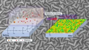
The approach investigated by the researchers was based on development of a method to generate, in a highly controllable manner, nanostructures having directional randomness and dimensional order. The nanostructures were produced on a thermally pretreated poly(dimethylsiloxane) (PDMS) surface after a short duration Reactive Ion Etching (RIE) treatment with Ar, O2 ions and electrons via physical bombardments and chemical reactions.
After the RIE treatment, the PDMS surface turned into a silica-like layer with a topography of sinusoidal undulations having a periodicity and depth distribution that ranged from dozens of nanometers to micrometers. The nanostructure was widely and homogeneously distributed over the entire surface. The process is illustrated in the graphic below.
 The reactive ion etching process that was used to generate quasi-periodic nanostructures.
It was found that an advantage of this approach was that the average depth and periodicity distribution of the nanostructures could be controlled by tuning the conditions of the pretreatment of the PDMS and the RIE processing parameters. In addition, the researchers demonstrated the ability to independently tune the average depth and the dominant periodicity of the undulations.
When these nanostructures were integrated into a two-unit tandem white OLED device, a maximum external quantum efficiency of 76.3% and a luminous efficacy of 95.7?lm/W were achieved with extracted substrate modes. An enhancement factor of 1.53?±?0.12 at 10,000?cd/m² was obtained.
In order to better understand these results, the researchers developed an optical model to explore the mechanism behind the nanostructure generation and controllability.
The optical model considered the dipole position and dipole orientation as well as the emitted wavelength and simulated device performance by dividing the nanostructures into sinusoidal textures with a dominant periodicity and height. Based on these models, it was found that the generation and controllability of RIE-induced nanostructures could be explained by the theory of thin-film deformation in a planar bilayer system.
More specifically, it was determined that “layered thin materials generate mechanical deformations such as creases, wrinkles and undulations on the surface in response to small compressive stress release between the top stiff layer and the bottom soft base, induced by thermal, light, mechanical or osmotic stimuli. Deformations arrange randomly in directions and amplitude, accompanied with in-plane stress release on the entire surface.”
The researchers state in the conclusion of their article that the use of RIE-induced nanostructures in white OLEDs demonstrated the ability to efficiently extract waveguide modes and surface plasmon polariton modes leading to a higher efficiency, together with improved color stability and more homogeneous radiance distribution. They go on to state that, since the controllable generation of these nanostructures is lithography-free and scalable to large surfaces, it follows that the process should be cost-effective in industrial use. Furthermore, because nanostructures can be directly generated on the PDMS surface, they are compatible with emerging flexible devices. -Arthur Berman
Technische Universität Dresden, Sebastian Reineke, +49-0351-463-38686, [email protected]