Nanophotonica is a company that has already gotten the attention of many display developers, but they have not been too visible beyond their development partners so far. That may be changing as I recently had a chance to talk with Chris Morton, CEO of the company.

They appear to be doing some impressive work in developing an electroluminescent quantum dot (EL-QD) display solution that includes the full stack – not just the quantum dots. They even have impressive material lifetimes – one of the key challenges with EL-QD displays.
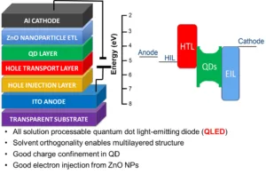
In our conversation, Morton explained that working the full display stack, which includes hole and electron transport layers, QD materials, electrodes, encapsulation, substrates and more, is extremely important if you want to be successful. The basic stack for an EL-QD display is shown below.
These layers are similar to what is needed with OLED displays, but Nanophotonica is pursuing an inkjet printing approach for their device manufacture. Development of ink jet printing of OLED displays has been on-going for probably a decade, but to my knowledge, no mass production facilities are yet up and running. Nevertheless, Morton says they can take advantage of all that development work to help move toward mass production.
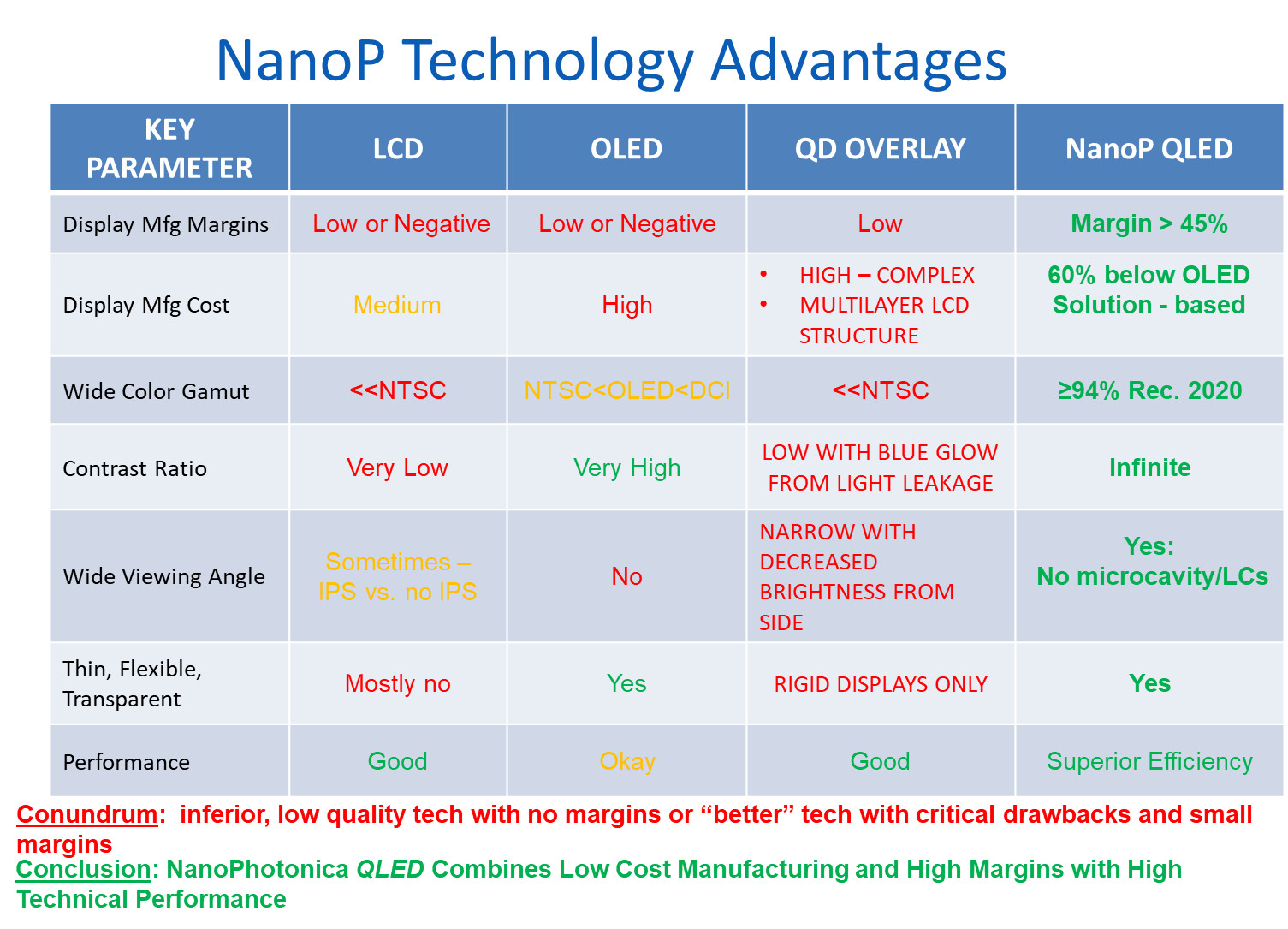
Many think EL-QD displays offer the potential to give OLED-like performance with LCD-like pricing (some think the same thing of microLED displays). But we are still far from proving that. Nevertheless, the chart below suggests how Nanophotonica views the EL-QD display opportunity.
So how good are their QD materials? Morton says they have developed both Cd-based and Cd-free quantum dots, but Cd-free will be preferred by many (except for China, many suspect). While exact lifetime and quantum efficiency numbers are confidential, Morton claims they are impressive and state of the art in both Cd-free and Cd-based systems. As for color gamut, DCI-P3 is easily obtained and they have demonstrated samples to 94% of the BT-2020 color gamut.
In terms of pixel density, they have shown 200 ppi already and have a plan to go to 300 ppi. These are pixel densities that can enable a 75” 8K TV, for example. Phones need pixel densities in the 500-600 ppi range, which will be much harder to get to, but they have a new pixel architecture they hope can get there, which Morton could not elaborate on.
Going Commercial?
Are these numbers good enough for a commercial product? Morton was a little more elusive on this as they are engaged with a number of customers looking at a number of products – and even in the same product category there is no agreed upon requirement for the material specifications. He could not disclose much about the partners they are working with or the product categories, but he did say that everyone is interested in the TV category and he thinks together, they can be close to producing a TV in about two years. Samsung is on record as being an investor in the company, but Morton suggested that other major players are also engaging with them.
Clearly, there is a lot of work to do over the next two years, but Morton sees their materials for ink jet printing solution being ready for mass production by the end of 2019. Qualification of materials and processes will then have to commence along with considerations of second sources and other supply chain issues. Producing millions of anything requires a lot of planning and development.
Morton says their business model is to develop the materials and processes for the full display stack and to then partner and license to manufacturing partners with a revenue share on materials sold. They are already engaging with bigger materials and manufacturing partners to get these pieces in place.
Nanophotonica seems like a company to keep tabs on. – CC