In the afternoon session, the focus was more on advanced 3D displays. Jon Karafin from Light Field Labs started the discussion by giving a presentation most of which we have described before. It included a discussion of what he views as a light field display and what is not a light field display. Many of the 3D displays in movies are not possible, of course, and he says that a true light field display in a head mounted display is not really possible either.
Light Field Labs is developing a tiled-based light field display that can be used for larger-sized display solutions in museums, theme parks and maybe cinemas. The current display module is 6 inches (15cm) wide and offers 16K x19K pixels, which are used to create light rays in many directions. How it does this is not disclosed. His roadmap calls for commercialization in the 2020 time frame and he even hinted at technologies that may allow interaction for the light field display in the future as well.
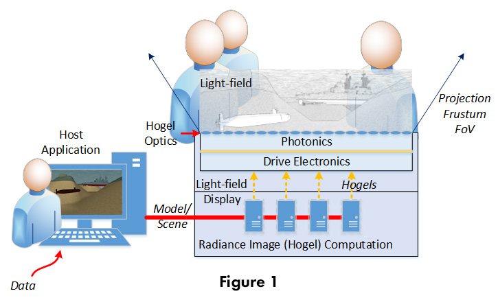
Samuel Robinson from Holochip used his time to describe some of the LF display projects they are working on. He divided their efforts into single user and multiple-user projects. Single user displays are less challenging as they can have smaller screens, smaller FOVs and a smaller radiance image resolution. A radiance image can be presented as a 2D image where each pixel represents the color, position and direction of a ray within the light field.
Single user LF displays can use currently available GPU cards (limit 8K per card). The 3D display from JDI, the Leia LF display in the Red Hydrogen phone, LF HMD prototype from nvidia and a flight simulator are all current examples. Robinson said they are working on a helicopter flight simulator for the “chin window” where 3D depth perception is critical for landing, and working with Red and Leia.
Multi-user applications include themed entertainment, cinema and command tables. Here, the FOV, screen size and radiance image all need to be much bigger. This requires new processing architectures and clever ways to deliver data to the LF display.
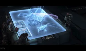
The photo shows an artist’s rendition of a future command table. Note that this is not practical as shown as light rays must emanate from the display surface and intersect the eye to be physically realizable so some of the images above the table do not meet this criteria. If the display surface was placed at the floor level, then more of the image would be visible.
Robinson says they have a contract to develop a LF command table for the Aegis Destroyer, but they are taking a very practical approach to building it. While it needs to support a multi-gigapixel radiance image, they are using a Lambertian shading model to simply calculations. Nevertheless, it does require a custom multi-CPU/GPU solution.
Thomas Burnett from FoVI3D provided more details on their vision of a heterogeneous display ecosystem. He defines the light field Hogel as “The combination of micro-lens and micro-image. The micro-image colors rays emitting from a point spot on the image plane and the micro-lens angularly distributes the light-rays.”
Burnett explained that there are two traditional approaches to computing the radiance image: double frustrum and oblique slice and dice. Each has their advantages and disadvantages and they use both methods depending upon the display device and other factors.
Computation of the radiance image needs to be done for each hogel and some of the displays the FoVI3D is working on have 50×50 arrays of hogels. Traditional GPU pipelines render each view in a sequential manner. That means the 502 rendering thru the GPU to create just one image. That is not practical, which is why Burnett is calling for a massively parallel approach to computing the radiance image – a heterogenous computing environment.
Like Third Dimension Technologies, FoVI3FD is suggesting a modified OpenGL source code is the way to deliver content that can be played back on multiple types on 2D and 3D displays using only a single source. They are developing an Object Graphic Library for OpenGL (similar to TDT) that would be combined with a parallel computing environment. Their MvPU (Multi-view Processing Unit) concept tries to assign a GPU/CPU to as few hogels as it can to speed up processing.
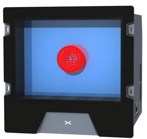
FoVI3D also showed their latest LF display at the event. Called DevKit Lucas, details are described in the graphic below. This is still a monochrome image with about 4 inches of useable depth before it gets too blurry to be useful. But, the image calibration has improved so that the lines between display module are now greatly reduced leading to a more uniform image with fewer artifacts.
Switching gears to cover volumetric displays, Ilmars Osmanis from LightSpace Technologies described their technology. It is based on a DLP engine that flashes slices of a 3D data set that are sequentially displayed on a series of diffuser sheets composed of their specially manufactured LCDs. The commercially available model (X1406) is a 19.5 inch monitor with 20 physical depth planes with a 4-inch deep image. It creates an image with 1024 x 768 x 50 voxels of resolution.
A 27” version of this monitor (x2701) is in development and will have 5-6 inches of depth volume offering a resolution of 2560 x 1600 x 40 voxels using 16 physical diffuser planes.
Osmanis also described the development of a benchtop display that will have a 39” diagonal and a 5 inch depth volume. Voxel resolution will be 2048 x 1539 x 40 using 8 to 16 physical image planes. They even are developing a 54” version with a 6 inch depth and 5120 x 3200 x 40 voxel resolution.
Finally, Osmanis described a project to develop an HMD based on the volumetric concept. He admitted this will be “like a toaster on your head” suggesting it will be big and bulky, but they hope to reduce it if performance is good.
LightSpace also showed the 19” model at Display Summit. Images looked quite good due to a new double off-axis DLP engine design that reduces the black level by 100X. It has decent spatial resolution although update rates seemed slow. It was also able to be driven using the ObjGL language that FoVI3D is developing to prove that the concept works.
The last speaker of the day was Vladimir Matias at iBeam Materials. His company works closely with Sandia National Labs where they leveraged thin metal foil technology used for superconductors to develop a novel microLED approach called GaN-on-Metal. This could be quite a breakthrough in LED/microLED fabrication as it may transform how LEDs are made and used.
The key is an ion-beam processed crystal alignment layer that sits between the metal foil and the epitaxial growth layer of GaN. The process is shown below.
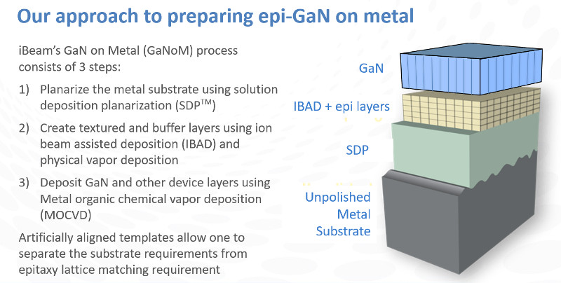
The Ion Beam Assisted Deposition (IBAD) process is used to align the grains in the epi layers to create a single-crystal-like layer for MOCVD GaN growth. Matias says the process is extremely fast aligning the grains in 1 second with a less than 5nm epi layer. 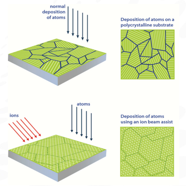
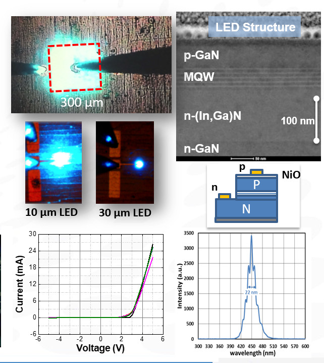
Key benefits include a much improved heat sink for lower device temperatures, better wavelength uniformity so no binning needed, plus the metal foil is a natural reflector for better light extraction. The first blue LEDs have demonstrated a 70% IQE from photoluminescence. LED devices as small as 10 microns have been fabricated and a bend radius of 7mm is possible too.
What’s really cool is that this now creates the possibility of making GaN devices in a roll to roll process on metal foil. This can revolutionize not only microLED fabrication, but could be used for LEDs for all kinds of applications. Think flexible LED displays.
While it still early to be forecasting the cost of production, Matias thinks this R2R process can be much less expensive than planetary deposition systems used in GaN wafer fabrication today. The cost per area depends heavily on the width of the R2R web tool, but his model suggests GaN deposition costs of $0.32 per cm2 for a 10cm wide web and a mere $0.07 per cm2 for a 100cm wide web. That would make it cost competitive for a microLED cellphone display compared to OLED.
MicroLED devices can be made directly on this GaN substrate as transistors and emitters can both be made with the materials. Black photoresist would cover these parts while patterning of quantum dots would be needed for red and green. A color gamut in excess of DCI-P3 has already been shown.
If this can be commercialized, it may offer a path for low cost pixels at high density – exactly what is needed for light field displays. – CC