We have mostly reported on Lattice Semiconductor in its capacity as the buyer of HDMI developer, Silicon Image. However, now that the companies have combined their technologies, they have a new class of chip, designed to solve problems for engineers that need to be able to support multiple display and capture interfaces – a ‘bridge’ chip. Lattice’s Grant Jennings told us that the new CrossLink chip family architecture uniquely combines the advantages of the flexibility of FPGAs with the speed and cost performance of ASICs or ASSP (Application Specific Special Processor). We had a phone conversation with the firm to better understand what the chip is for and more about this ‘best of both worlds’ claim.
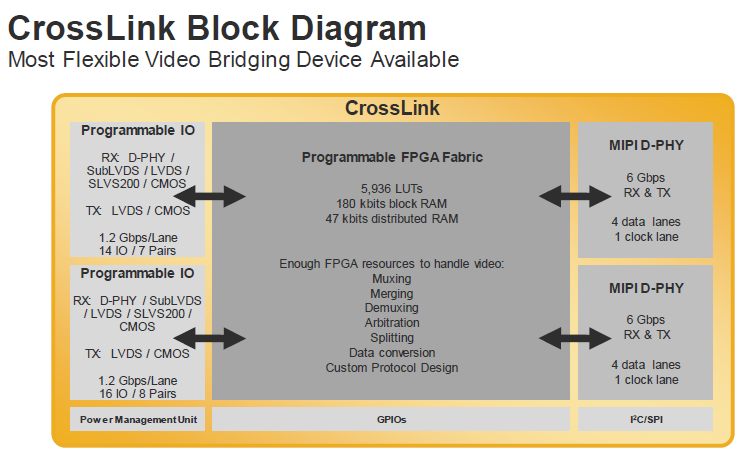
One of the claims by Lattice is that there is no downside to the combination of approaches. We were surprised at this, but it seems that on this kind of chip, the size is ‘pad limited’ that is to say that there are so many connections needed that this is the factor that sets the silicon size and cost. Effectively the chip has to be bigger than it might be if there were no connections. The FPGA part of the chip can be re-programmed from a CPU or by a traditional external programmer.
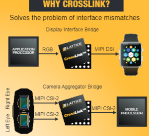
The CrossLink device is intended to support a wide variety of interfaces in applications from VR, drones, cameras, wearable devices, mobile devices and human machine interfaces. To get the speed and economy needed to support multiple high bit rate interfaces, the chip includes a number of blocks that can perform common processing functions.
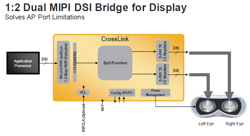
The chip is claimed to be the fastest MIPI -PHY bridge that can offer up to 12 Gbps for 4K UltraHD resolution. However, it can also support MIPI CSI-2, MIPI DSI, MIPI DPI, CMOS, and SubLVDS, LVDS and more. It can work in cameras and displays to support multiple streams – for example the dual displays of VR headsets which typically need to be driven from a single application processor.
At the same time, it has small size (6mm²) and low power. In a call with the company, we heard that the chip can be set into sleep modes and directly woken without resetting, which means power saving can be sophisticated. The company has also developed a number of optimised solutions that are available for known configurations which means a quick development process for many clients. An example would be for bit depth conversions. To help developers, Lattice has worked on boards to allow dual cameras to be used on the Raspberry Pi.
Evaluation boards are available now and sampling will start at the end of Q2. (BR)