Origami (making 3-D shapes by folding paper) and kirigami (which allows cutting as well as folding) are ancient arts. Nano-kirigami has taken off as a field of research in the last few years, targeting not centimeter-sized pieces of paper but micron-sized flat materials with individual features at the nanoscale.
![]()
Researchers in the US and China working under Massachusetts Institute of Technology (MIT) Professor of Mechanical Engineering Nicholas X Fang recently reported on a simple single step process that allows making of complex and useful optical shapes using this nano-kirigami techniques.
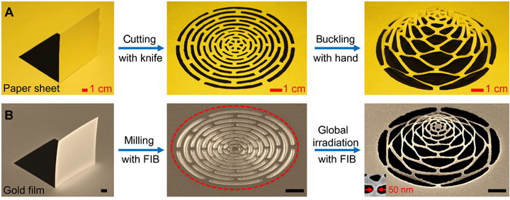 (A) Camera images of the paper kirigami process of an expandable dome, a traditional Chinese kirigami named “pulling flower.” (B) SEM images of an 80-nm-thick gold film, a 2D concentric arc pattern and a 3D “pulling flower” microdome. The high-dose FIB milling corresponds to the “cutting” process, and the global low-dose FIB irradiation of the sample area (enclosed by the dashed ellipse) corresponds to the “buckling” process in nano-kirigami. A 3D feature size of 50 nm is shown in the inset. The scale bar in each nano-kirigami image is 1µm. (Credit: MIT)
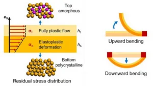
The technique involves writing the patterns on a very thin (80nm) thick gold film with a focused ion beam (FIB) composed of gallium ions. At high doses, this FIB cuts the material. With lower doses over larger areas, the stresses in the film shape the material into complex 3D shapes. Some of the stress comes from the two layer (amorphous and polycrystalline gold) structure of the film the researchers used plus there is additional stress induced by the implantation of the ions in the FIB. These stresses are very predictable, however, so the researchers can predict what shape the film will fold into after being cut.
This was a problem with previous research into nano-kirigami – it was not possible to predict the final 3D shape the film would form after being cut and, therefore, it was trial-and-error to make the desired shapes. In addition, previous nano-kirigami processes were multi-step, requiring more than one production environment. In the MIT process, there is only one environment with the FIB both cutting and shaping the nano-patterns in the material.
Left: The two-layer gold film used by the researchers. Right: When the film is cut around three sides as a freestanding “finger,” the finger bends up. When cut along two sides with both ends supported, the film bends down.
These shapes are extremely small and electromagnetic radiation in the visible and IR ranges see them as single elements, not as complex 3D shapes. Depending on the shape generated, the technology can be used, in theory, at least, to generate virtually type of dichroic filter, including AR coatings, wavelength filters and polarizing films.
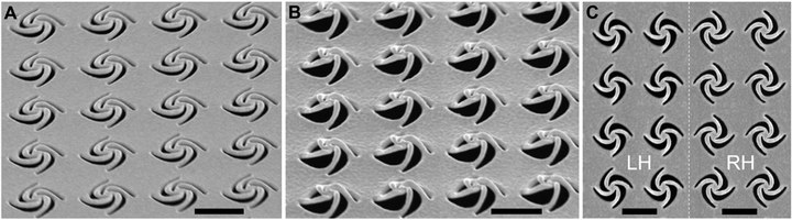 (A and B) SEM images of (A) 2D and (B) 3D pinwheel array with periodicity of 1.45 ?m. The height of the 3D pinwheels is about 380 nm. (C) Top-view SEM images of left-hand and right-hand 3D pinwheel arrays. Scale bars, 1 ?m. (Credit: MIT)
For this article, the researchers focused on a type of surface that is difficult or impossible to produce with traditional dichroic filter technology: chiral layers that act as circular polarizers, as shown in the image. The paper presents data showing that the calculated behavior of these structures in optical applications closely matches the measured optical properties. The authors point out that electromagnetic theory requires that any structure showing chirality, such as a circular polarizer, must have a 3D structure. The 2D pinwheel structures in part A of the image above only show chiral properties off-axis, where the light beam encounters different parts of the structure in different 3D planes. The 3D pinwheel structures of nano-kirigami in parts B and C of the image also show chiral properties at normal incidence, in accordance with theory.
In conventional systems, chiral liquid crystal (LC) materials can be used to make circular polarizing films, although these layers typically have rather narrow bandwidths. They are also subject to thermal and lifetime problems associated with the organic LC materials. Conventional circular polarizers are typically at least two layers, a linear polarizer and a retarder to convert linear polarization into circular polarization. This technique, for example, is used for the 3D glasses used in most cinema 3D systems. For high powered applications, such as at the projector in 3D cinema, a complex (and expensive) system of reflective polarizers, mirrors and retarders is used to convert the unpolarized output of the projector into circular polarized light for projection.
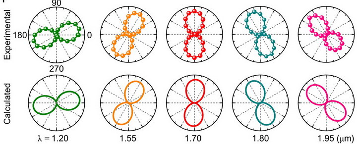 Experimental vs Calculated optical properties of the pinwheel arrays. (Credit: MIT)
The 80nm thick gold film used was supported by a mesh of copper with a 100µm x 100µm pitch. This limited the largest element or array of elements MIT could fabricate to a 100µm by 100µm square. While the authors used a gold film for this paper, they say the technique will work in a wide variety of suspended thin-film materials and they have tested it with aluminum and commercial silicon nitride thin films. The silicon nitride film required a very thin layer of gold, presumably to make it conductive. Of course, the finite-element elastoplastic mechanical model used to predict what shapes will be formed by a given cutting pattern must be adjusted for the properties of the aluminum or silicon nitride films.
MIT has put a video on YouTube showing the fabrication of these nano- kirigami elements. This research was supported by the National Key R&D Program of China, the National Natural Science Foundation of China, and the U.S Air Force Office of Scientific Research. Nice to see some US/Chinese cooperation even for technology that the US Air Force sees as having military potential.
While this particular paper discusses only static structures, it is also possible to make nano-kirigami elements dynamic. In micro-electro-mechanical systems (MEMS), such as the DLP from TI, multistep processes including many photolithographic mask steps and etching processes are used to produce the elements. Professor Fang pointed out that the nano-kirigami elements were produced essentially by a single step using the FIB, initially at high intensity for cutting the film and then at lower intensity to induce the desired bending. This simple processing could lead to an entirely new field of nano-electro-mechanical-systems (NEMS).
Professor Fang pointed out the research is still at an early stage, so more research will be needed on possible applications. But these devices are orders of magnitude smaller than conventional counterparts that perform the same optical functions, so these advances could lead to more complex optical chips for sensing, computation, or communications systems or biomedical devices, the team says.
Displays are probably a very long term application of this technology – years away at least and more likely decades. One of the limitations is fabrication time: For an array of 3D pinwheels with lattice period of 1.45 ?m and sample area of 30 ?m × 30 ?m, the fabrication time was a little less than 30 minutes. Professor Fang mentioned two shorter-term applications.
First, a sensor could be designed that separated left and right hand circularly polarized light. This could be used in a glucose sensor to detect the left and right hand sugars in the solution individually. This would be important because left and right hand sugars have different medical implications.
Another application would be to multiplex left and right hand light into a single fiber for data transmission applications to double the data capacity of the fiber. That is why the pinwheels in the above image have a 1.45µm pitch – this is a common IR wavelength for data transmission. For these high-value applications, perhaps the fabrication time isn’t a problem.
This paper is available for downloading for free at Nature’s Science Advances website. Additional information is also on the MIT website. –Matthew Brennesholtz