
Researchers at the University of California, Irvine, have developed a mechanically reconfigurable nanoscale electronic devices using van der Waals (vdW) layered materials, which have low interfacial friction. Traditional electronic devices are static, meaning their material structure and geometry are set during fabrication and cannot be changed afterward. To explore different configurations, multiple devices with varying geometries and material structures have to be made.
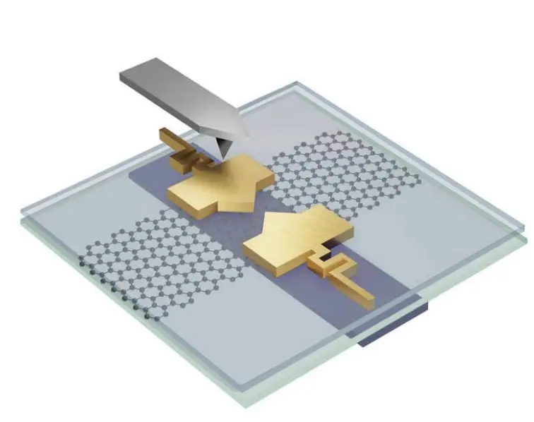
Microelectromechanical systems (MEMS) provide some mechanical reconfigurability, but with limitations due to complex suspended device structures. Van der Waals materials, like hexagonal boron nitride (hBN), offer a solution because they have low friction between layers, making them easier to slide and reconfigure. Unlike conventional MEMS, the sliding-based approach in this research does not require suspended components, which could make the fabrication process easier and the device more robust overall.
The authors demonstrate that gold also exhibits low friction when sliding on hBN at both ambient and cryogenic temperatures (7.6 K). This property allows the creation of a variety of mechanically reconfigurable vdW devices, such as tunable graphene quantum point contacts (QPCs) and sliding-based scanning probe devices. These devices can be modified after fabrication, either ex situ using an atomic force microscope (AFM) or in situ in a measurement cryostat (a device used for maintaining low temperatures). Potential applications for these reconfigurable devices, which are similar to those of conventional MEMS devices, include electromechanical switches, accelerometers, micro-positioners, and optical beam steering.
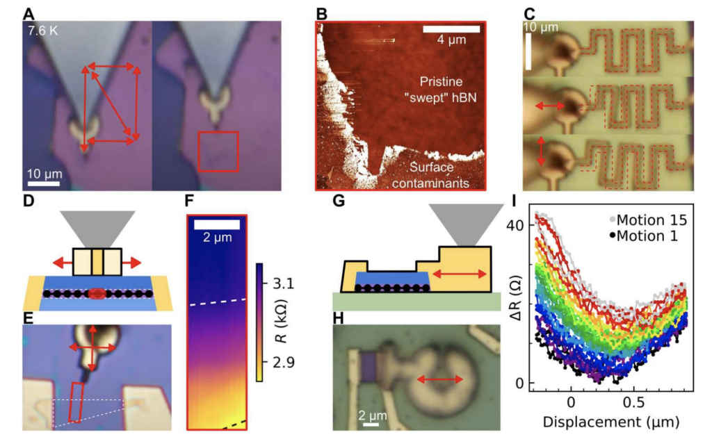
(A) The optical images display gold moving on a pink hBN (hexagonal boron nitride) surface at 7.6 K, pushed by an AFM (Atomic Force Microscopy) tip. Arrows show the motion range and direction. The dark purple area on the left is the SiO2 (silicon dioxide) substrate. A video of this motion can be found in movie S1. (B) The AFM image reveals the hBN surface remains undamaged after the cryogenic scanning motions from (A), with only surface contaminants gathered. (C) Optical images show gold serpentine electrodes on hBN, exhibiting about 2-micrometer movements in two directions. Red dotted lines mark the initial position. Videos of the oscillating motion are available in movies S2 and S3. (D) A side profile illustration displays a sliding top-gate hBN-encapsulated graphene device moved by an AFM tip. The top-gate slides over stationary graphene, changing local gating and device resistance. (E) A top-down optical image of the same device, with graphene outlined in a dotted white line and a light purple background of hBN. The red rectangle measures 2.4 x 9.5 micrometers. (F) A graph shows graphene resistance versus the top-gate position, with scanning range represented by the red rectangle in the optical image. Dashed lines indicate graphene edges. (G) A side profile illustration of a slidable graphene-hBN device on a stationary hBN substrate, moved by an AFM tip. The slidable features in the schematic are outlined in black. (H) A top-down optical image of the same device, with a pale green background of hBN. (I) A graph shows the two-probe resistance of the slidable graphene device versus its sliding position. The initial position corresponds to 0 micrometers. The increase in resistance over subsequent motions is likely due to photodoping from the light source used for imaging.
UDC has a patent for a hybrid OLED using a blue light LED where the shutter element positioned between the backlight layer and the frontplane can be a MEMS device or an LCD. In this patent, the shutter controls the intensity of transmitted blue light by amplitude modulation or pulse-width (time) modulation. There are other display applications of MEMS, for example, traditional tactile displays employ large-sized actuators and offer poor resolution in conveying tactile sensations, however, MEMS technology enables the fabrication of miniature structures, enhancing the performance of tactile displays.
Reference
Mechanically reconfigurable van der Waals devices via low-friction gold sliding | Science Advances. (n.d.). Retrieved April 30, 2023, from https://www.science.org/doi/10.1126/sciadv.adf9558