A team of researchers headed by Yutao Qu of the Department of Electrical Engineering and Computer Science at the University of Michigan (Ann Arbor, MI) are developing a microlens array based means for increasing the efficiency of light extracted from OLED devices.
A recent article on this topic by the team is entitled “Efficient, Nonintrusive Outcoupling in Organic Light Emitting Devices Using Embedded Microlens Arrays.” The article was published on-line in ACS Photonics on April 17th. A copy of the article is available for purchase here.
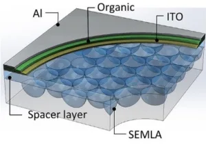
Called a Sub-Electrode MicroLens Array (SEMLA), the array consists of a flat spacer layer on top of a hexagonally closed packed array of 10μm diameter hemispherical lenses. In a device, the microlens array is embedded between the OLED’s bottom transparent ITO electrode and the glass substrate. That is, the SEMLA is “internal” to the OLED device.
The microlenses were designed using ray tracing calculations. Parameters input to the calculation included several that related to the configuration of the device. Such parameters included a 40 nm ITO anode, a 40 nm hole transport layer, a 20 nm emission layer, an electron transport layer and an aluminum cathode.
The calculations indicated that the light extraction from the internal SEMLA into glass is more efficient than from an external microlens array into air. An external microlens array can be thought of as a more conventional approach. The improved extraction is due, in part, to reduced reflection at the lens/glass interface since the critical angle is larger in a configuration with an internal SEMLA microlens array.
In their recent article, the researchers go on to report the fabrication of a prototype device by mating a SEMLA with a bottom emitting phosphorescent OLED. A few of the details of the implementation are as follows: “a high refractive index, non-diffractive hemispherical microlens array was located between the transparent anode and embedded in the low refractive index glass substrate (n = 1.5). The refractive index of the lenses in the SEMLA was chosen to be 1.8, close to that of the organic layer and the ITO electrode.”
The figure below illustrates the configuration of an OLED stack on top of a SEMLA substrate.
An OLED stack built on top of a SEMLA substrate.
The performance of the prototype device was then evaluated. The researchers report “an external quantum efficiency of up to 70 ± 4% for green phosphorescent OLEDs and up to 50 ± 3% for white phosphorescent OLEDs. These values indicate that the light output was enhanced by a factor of 2.8 and 3.1 compared to similar devices built on conventional glass substrates.”
Clearly, the SEMLA approach was a very effective means for extracting light trapped in the active region of the OLED. It was further demonstrated that the SEMLA structure provided enhanced light extraction that was wavelength independent.
The researchers make special note of several features of the SEMLA approach.
- Since the SEMLA is external to the device active region, it does not affect the actual design of the OLED itself.
- The surface of the SEMLA is smooth. As a consequence, there is little optical scattering related to the SEMLA structure. Given this fact and the fact that the SEMLA layer is quite transparent, no decrease in image sharpness was apparent when SEMLA was included in the OLED display.
- The SEMLA approach can be used with regular glass substrates in place of conventional sapphire substrates. As a result, manufacturing costs can be reduced.
- Due to the micrometer scale feature size of the SEMLA, it is possible to fabricate the array using conventional photolithography prior to the OLED array deposition. This is a second reason why the SEMLA approach can be inexpensive to implement.
The researchers see the SEMLA approach as potentially suitable for both display and lighting applications. – Arthur Berman
University of Michigan, Yutao Qu, 734-936-0069, [email protected]