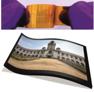
Researchers from the Indian Institute of Science’s (IISc) Department of Materials Engineering have fabricated a highly flexible, composite semiconductor material. This news is positive PR for India’s continued push to be a major player in semiconductor and display manufacturing, after the turmoil in the relationship between Foxconn and Vedanta, a flagship, high-profile display venture locally.

Semiconductor devices such as transistors, the fundamental building blocks of electronic circuits, typically consist of amorphous silicon or amorphous oxides. Their inherent rigidity and low strain tolerance limit their adaptability in modern, flexible electronic applications. One common approach to augment flexibility has been to incorporate polymers into oxide semiconductors. Yet, the trade-off has always been a compromise in semiconductor performance due to the limited quantity of polymer that can be added.
In a departure from previous research, which reported polymer additions of only 1-2%, the IISc team managed to incorporate up to 40% polymer into their composite. This high polymer content, integrated using a solution-process technique — inkjet printing, in particular — didn’t affect the oxide semiconductor’s functionality. The composite semiconductor remained as capable as ever, with the added advantage of extraordinary flexibility and foldability.
Composed of a water-insoluble polymer (ethyl cellulose) for flexibility and a semiconductor (indium oxide) for excellent electronic transport properties, the composite semiconductor displays a unique phase-separated structure. The team designed the material by mixing the polymer and oxide precursor to create a network of interconnected oxide nanoparticle channels around polymer islands. Electrons can traverse these channels from one transistor end (source) to the other (drain), thereby ensuring a consistent current flow.
According to Subho Dasgupta, Associate Professor at the Department of Materials Engineering, this strategic design enabled the creation of a super flexible composite semiconductor. The phase-separated, polymer-rich islands arrested the formation of cracks, a feature essential for flexibility.
The IISc team, led by Dasgupta, broke away from conventional semiconductor fabrication techniques such as sputtering and instead used inkjet printing to deposit their material onto a variety of flexible substrates, including plastics and paper. The current study used Kapton, a polymer substrate. This printing approach, despite its challenges — from achieving a homogenous film to managing the ink’s printing conditions — lends itself to widespread application.
Dasgupta believes these printed semiconductors will find their place in fully printed and flexible televisions, wearable technology, and large electronic billboards, along with printed organic light-emitting diode (OLED) display front-ends. Given the ease and low-cost nature of their manufacture, these printed semiconductors hold the potential to revolutionize the display industry.
The research team has secured a patent for their groundbreaking material and are gearing up to evaluate its shelf-life and device-to-device quality control before scaling up for mass production. Concurrently, they’re exploring alternative polymers that could help design such flexible semiconductors, marking an ongoing commitment to advancing flexible electronics.
Reference
Divya, M., Cherukupally, N., Gogoi, S.K., Pradhan, J.R., Mondal, S.K., Jain, M., Senyshyn, A. and Dasgupta, S. (2023), Super Flexible and High Mobility Inorganic/Organic Composite Semiconductors for Printed Electronics on Polymer Substrates. Adv. Mater. Technol. 2300256. https://doi.org/10.1002/admt.202300256

