 OTI Lumionics was next up and the speaker was Michael Helander who is the founder and CEO. The company focuses on the electrode materials to help with manufacturing, which is an under-served market. The same materials from twenty five years ago are still being used, but bottlenecks are starting to appear. The company is working with OLED makers and equipment makers.
The company uses analytical simulation on CPUs and GPUs for checking materials for their potential as electrodes. The company uses external chemists for evaluation and then tries pilot production. Often the conditions in a fab are very different from a lab, so this testing avoids problems when materials go into mass production. The company can also test with customers in real products. New materials often fail in different ways from traditional products.
There have been issues with burn in and high power consumption in OLEDs and there are no large OLED panels with top emission at 55″ and above. There is clear demand for OLEDs in notebooks and even monitors that were shown at CES in 2016, but they had been cancelled by CES in 2017 (including the Dell monitor).
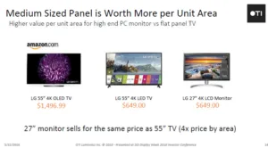
OTI believes there is a big opportunity in mid-sized displays, although TV is, of course, the largest market. There is a large segment of the market that OLED simply can’t address. However, if you look at 27″ monitors, they are often the price of 55″ TVs so the revenue per square metre is much higher for monitors (we haven’t heard that said for a while -IT panels always used to be ‘poor relation’!)
IT panels are no longer the ‘poor relations’ and products are more valuable than TVs. Image:Meko
So why do we have nothing in between? TVs use white OLED with bottom emission with less than 100ppi, while smartphones are at high ppi and use top emission. In the top emission architecture, the electrode has to be transmissive and conductive. Even TV, however, is trying to move to top emission to get higher resolution to support 8K and needs better power consumption. All current forecasts from analysts are assuming top emission.
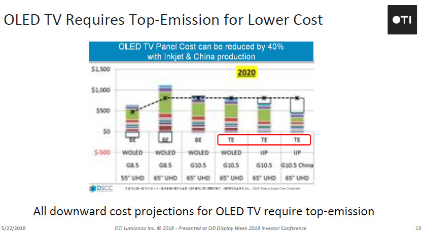 OLEDs will need top emission to succeed in the market.
However the dirty little secret of the OLED business is that at the moment, the top electrodes are not suitable for large displays. The resistance of the cathode becomes a big issue for large displays with a 2.X V drop on a 15″ (check slides) from the edge to the middle.
OTI has a new material that it calls ConducTorr that allows large displays to be made. Unfortunately current patterning techniques don’t work when performed on top of the OLED structure. So the ConducTorr material has been developed to be depositable via mask, UV, prointing or laser. The company has used light activation and also FMM down to 6.5 µm. The company can get the resistance down by a factor of 100 and can also allow a range of choice in transparency, it claims. The company said it has demonstrated the materials in a 5.2″ panel using existing mask and vacuum processes. In the demo, Helander claimed, there were no defects from the electrode (although there were some backplane defects).
The company is ready for mass production and will have volume materials in Q3 from the firm’s manufacturing partner and it can fine tune the technology for different applications.