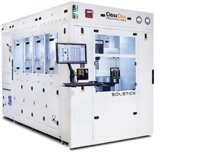
ClassOne Technology announced it has received a follow-on order for its Solstice GoldPro gold electroplating system from a leading microLED maker with global manufacturing sites. Built on ClassOne’s state-of-the-art Solstice platform, the system will be used at the customer’s new manufacturing site in Asia for high-volume production of next-generation microLEDs deployed in a range of end applications.
ClassOne’s Solstice S8 system features the company’s proprietary GoldPro plating reactor. Designed to provide efficiency, speed, and improved cost of ownership, GoldPro leverages ClassOne’s unique fluid motion profile technology to deliver high plating rates and industry-leading plating feature uniformity. The Solstice S8 is on target to ship for installation in the second quarter of 2023.
“Its latest order is evidence of our customer’s success with its existing base of tools, pointing up a significant partnership between ClassOne Technology and this major microLED player,” stated John Voltz, senior vice president of global business operations for the company. “This customer views the Solstice platform’s capabilities as key to accelerating market-readiness for its devices, further validating our world-class single-wafer processing capability and technology leadership in the microLED space.”
According to Allied Market Research, the global microLED market is projected to reach US$23 billion by 2030, gaining ground over OLEDs by delivering improvements in brightness, contrast and energy savings. As a leading provider of plating equipment for microLEDs, ClassOne is well positioned to take advantage of this growth given Solstice’s high plating rates and throughput, strong customer base, and the addition of surface preparation processes to the platform’s already robust capabilities.
Available with up to 3, 4 or 8 chambers, the scalable Solstice platform is suitable for both R&D and high-volume manufacturing environments, delivering ultimate wafer uniformity and process control. The system can also accommodate a wide variety of substrates, from traditional silicon devices to compound semiconductors and emerging materials like glass.

