
Dutch deep-tech start-up FononTech has successfully raised €2.3 million ($2.6 million) in a seed investment round to further develop its innovative printed micro-electronics technology and pave the way for scaling up operations. The funding round saw the participation of five investors.
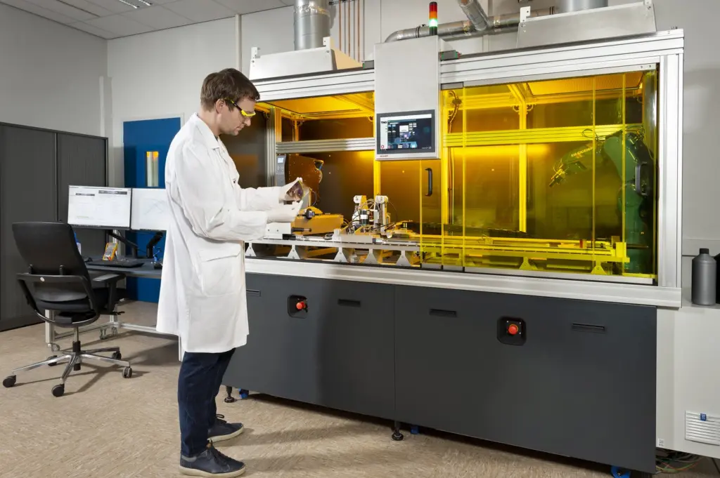
Micro-electronic components are continually shrinking in size and becoming more densely packed, often requiring intricate layered structures. The challenge lies in efficiently connecting these miniature parts together while ensuring enhanced performance and functionality in line with the demands of integrated electronics. FononTech’s CTO, Fabien Bruning, points out that conventional manufacturing techniques are reaching their limits in meeting these requirements. FononTech’s impulse printing technology (IPT) aims to surpass these limitations.
FononTech aims to focus on selling its core technology, specifically the printhead and filling mechanism, without the substrate handling component. This strategic approach aligns with their business model, as both the flat panel display (FPD) and micro-electronics markets require micromolds. CEO Rob Hendriks estimates that each mold produced by FononTech will last for a considerable number of “exposures,” ranging from a thousand to ten thousand, depending on the application. The company’s immediate goal is to develop a core system featuring a 128-by-128-millimeter printhead. With such a system, FononTech will have the capability to print panels measuring 600 by 600 mm, a format that is increasingly being adopted in back-end assembly processes. Moreover, FononTech’s system will also be able to print entire 300 mm wafers, further expanding its versatility.
In the FPD manufacturing realm, FononTech envisions its technology being employed for displays that use MicroLEDs, which are constructed by assembling numerous individual tiles. Here, IPT offers a distinct advantage: it enables the application of contact lines across the edges of the tiles, streamlining the assembly of large displays into fewer steps. Bruning emphasizes that traditional manufacturing techniques are reaching their limits in this domain, while IPT is poised to overcome these limitations.
One of the distinguishing features of IPT is its ability to substantially reduce the ecological footprint of micro-electronics manufacturing. Traditionally, lithography has been employed for chip interconnection, involving multiple complex steps with high carbon emissions that are difficult to mitigate. In contrast, IPT adopts an additive process, rapidly replicating patterns thousands of times while selectively depositing material only where needed. This eco-friendly approach has garnered considerable interest from the global semiconductor and display market.
The investors involved in this round include the TTT Smart Industries Fund, SHIFT Invest, Brabantse Ontwikkelingsmaatschappij (BOM), the Brabant Startup Fonds (BSF), and investor Sake Bosch. In addition to the seed funding, FononTech has secured a loan from Rabobank to support its operations.