Dawonsys (Ansan-city, Gyeonggi-do, Korea) has developed a new deposition process that has the potential for use in the mass production of OLED panels. Particular note is made of the fact that the process is reported as scalable to large sized panels.
First, a little background information.
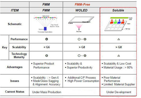 Image- based on source:Semi.org
At this time, two very different means have been developed with the capability to fabricate OLED panels.
- The first means is a solution-based process. This approach suffers from the fact that there is a lack of efficiency in currently available soluble luminous materials. These materials are also found to have limited lifetimes. This approach, therefore, does not currently lend itself to mass production.
- The second means is Vacuum Thermal Evaporation (VTE). This process uses a vacuum chamber in which the organic molecules are heated, evaporated and then condensed onto a cooled substrate. A very thin, Fine Metal Mask (FMM) is used to pattern the organic layer to form the subpixel structure.
VTE with FMM is the more mature and more used OLED production technology. None-the-less, it suffers from three major disadvantages.
- The majority of the organic material is deposited on the walls of the vacuum chamber or the mask, not on the substrate. While it is possible to recycle some of the materials, FMM still wastes a lot of material.
- It is difficult (though possible) to achieve a high resolution subpixel structure.
- The method is difficult to scale. One reason is that the mask is quite delicate. Larger masks tend to sag toward their center and, thus, lose dimensional accuracy.
This mask deflection effect has made it difficult to pattern RGB subpixels using three OLED materials on larger substrates since this process requires three, precisely aligned process steps. As a result, large OLED panels are commonly made using materials that emit white light used in conjunction with colored filters.
It should be noted that, as an alternative to FMM, Samsung has developed a technology that the company calls Small Mask Scanning (SMS). In this method, the mask is held fixed but the substrate moves. This allows the mask can be smaller since it does not need to cover the entire substrate.
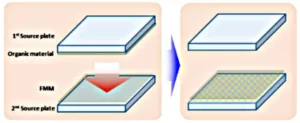
The new means developed by Dawonsys addresses the deficiencies of these previous approaches. It is based on Joule heating and a deposition that is directed downward.
In Joule heating deposition, a conductive film is coated on to a so-called first source substrate. A voltage is applied to the conductive film. Due to electrical resistance, the surface temperature of the film can be made to increase rapidly – even with the input of relatively little power. The hot conductive film is used to evaporate a thin film of an organic material that is coated on top of the conductive film.
In the Dawonsys approach, the first source substrate is positioned above a so-called second source substrate. The FFM is placed on the second substrate. The organic material evaporated from the first source substrate travels downward, is patterned by the FFM and then deposited on the second source substrate.
This process and configuration is illustrated in the figure below.
Dawonsys explained that, compared to point source or linear source evaporation, as used in conventional deposition process, the Joule heating deposition rate can be much faster at more than 100 Å/s. The efficiency of material usage is also quite high at between 70 and 80%. This is more than twice the efficiency of conventional methods. In addition, downward deposition is applicable to a large area FMM process. In fact, experiments have shown that the “shadow effect” dimension is 4um, which should enable high resolution deposition processes.
In conclusion, the new Dawonsys deposition technology should allow fabrication of a RGB subpixel structure in larger OLED panels through the use of the FMM process. Since this approach uses conventional deposition materials, it is expected that good efficiency and lifetime can be achieved. Hence, it is Dawonsys’ belief that the new deposition technology has the potential to play a role in large area OLED panel fabrication. -Arthur Berman