LEDs have been a hot topic in recent years in the display industry (pardon the pun) and there are interesting technical developments that are helping to drive the adoption of finer pitch LEDs.

The development of LED over the last fifty years or so has been a real triumph of engineering and science. In LEDs, the challenges have always included excessive heat, which has to be removed from the semiconductor chip itself, as it causes problems with lifetime and performance variation. The second issue in an LED is getting the light to go in the direction you want. Light comes out of the LED in all directions, but often the application needs more directed light.
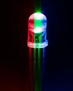
In the early days of discrete LED displays (and I do not refer here to TVs with LED-backlit LCDs that Samsung called LED TVs, causing confusion in the market, but to LEDs that are the pixel), the displays were made using individually packaged LEDs for each colour. LEDs chips were made with red, green or blue output. Each LED was individually packaged with some kind of heat sink to help to conduct away heat and a plastic lens that helps to manage where the light goes and to protect the LED from the environment. The package might contain a phosphor or other material to convert the colour of the light from the colour on the chip to the final colour desired. There were also wire leads attached to allow the connection to the driving circuit.
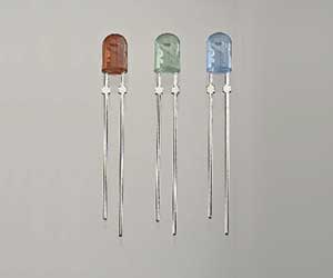 Cree’s C4SMK RBG 4mm Oval radial LED. Image:Cree
Now, this meant that the pixels could not be very close together, so displays could not be comfortably viewed from close up, although the different physical spacing of the coloured pixels could be used to do some clever sub-pixel addressing schemes, so for a while some companies talked about both the actual pitch and the virtual pitch, which was smaller. At least, the honest ones did!
The next move was to combine the three LED chips into a single package. By putting all three into one package, you could bring the pixel pitch much closer. Of course, you had, potentially, more thermal issues, but the control of colour balance and performance moved back up the supply chain to the LED packager, rather than being with the display maker. This change was really the beginning of the move to small pitch LED video walls.
SMD
The next development that allowed the current range of fine pitch right down to 0.8mm or 0.9mm was the development of Surface Mounted Device (SMD) LEDs. Rather than having wires coming out of the package, the LED package was developed to allow it to be simply soldered directly onto the substrate. The display can then be completed by ‘potting’ – there’s a great video from Osram showing the potting process that is used to embed the LEDs in the display. Moving to SMDs helped to drive down the cost of assembling LED displays as pick and place machines and fast soldering could be used and was a key part of moving to the state of the industry today.
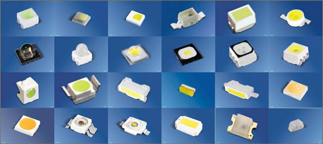 This shows the range of SMD LEDs. Source: Osram
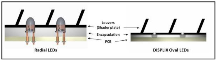 This image from Osram shows how the LEDs are mounted in outdoor LED displays. The louvres are fitted to reduce the effect of sunlight
CSP
The next stage, and the most recent change, is to move to Chip Scale Packaging for LEDs. This concept is based on the idea that if you can perform more processes in the semiconductor fab, this may be cheaper than doing them later (although there are those that don’t agree with this as they feel that the change just makes things harder for chip makers). At the moment, after you detach the LED chip from the wafer on which it was made, the chip still need processes that add a way of connecting to the substrate and also add some form of material that may help with heat dissipation (and there is work going on to develop better ways and materials to do this). Typically there will be a connection layer, an insulation layer and a thermal layer.
For applications that that require multiple LEDs, such as lighting, makers are putting multiple LED chips together onto circuit boards to create more powerful light sources. These are known as Chip on Board LEDs, but are not currently used in fine pitch LEDs.
 This Lumileds CSP LED has packaging the same size as the chip.CSP is an approach to add the packaging materials for heat management and connections are added at the time that the wafer is made. After this, the wafer is chopped up into chips and soldered to a high quality circuit board that can act as a heat sink. “Chip scale” literally means that the packaging is almost the same size as the LED chip itself. Better thermal performance means that chips can be run with more current, to achieve higher brightness. CSP LEDs can be efficient and Seoul Semiconductor recently announced a 2.2mm square LED for lighting that can produce 210 lumens/watt – a good level of efficacy that would have been ‘state of the art’ for a lab demo just a handful of years ago.
The improved thermal performance could be very helpful in getting the heat drawn away as effectively as possible from the LED, allowing smaller LEDs to be used (and with more of a black surround to improve contrast – Sony Cledis, anybody?)
Of course, the MicroLEDs that are attracting so much attention will be, almost by definition, CSP devices. To compete with current displays, microleds will have to have all of their processes completed with the scale and efficiency of semiconductor processing. There will be no room for separate processes. (BR)