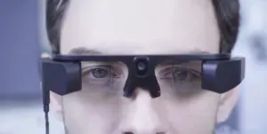
Core Vision Microelectronics, a developer of direct time-of-flight (dToF) chip technology, recently unveiled its latest offering: the global shutter BSI SPAD chip, VA6320. This latest stacked dToF depth sensor is a high frame rate, and low cost chip with potential applications in photography, AR/VR, and more. dToF is a method used for measuring the distance between a sensor (or camera) and an object. It operates by emitting a signal (often light or radio waves) towards the object and then measuring the time it takes for the signal to bounce back to the sensor after hitting the object. In the context of depth sensors in technology such as smartphones or AR/VR devices, dToF technology is used to map the environment in 3D. This information can be used for a range of applications, including augmented reality, gesture recognition, and improving the focus and depth-of-field effects in photography.
Core Vision compares the flash laser lighting technology in the VA6320 to Apple’s speckle technology. This refers to the use of speckle patterns in LiDAR (light detection and ranging) scanner, which is a remote sensing method used in Apple;s products, and many other applications including autonomous vehicle. The LiDAR scanner is used in devices like the iPad Pro and iPhone 12 Pro models for AR applications and to improve photography, particularly in low-light conditions and for depth sensing.
The LiDAR scanner emits laser beams (infrared light) that hit the objects in the environment and bounce back. When the laser beam hits the object, it creates a speckle pattern, which is basically the scattering of the beam due to the micro-irregularities of the object’s surface. The time it takes for the light to return is measured and used to calculate the distance each dot is from the LiDAR scanner, creating a detailed depth map of the environment. This speckle pattern is unique and allows for highly detailed surface recognition. Core Vision claims that flash laser lighting technology might offer certain advantages such as cost, size, and power efficiency.
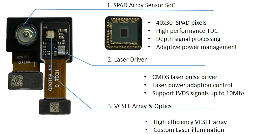
The real breakthrough feature of the VA6320 may be its 3D stack structure, which enables the sensor wafer and the image processing logic wafer to combine through a wafer-level Cu-Cu metal hybrid bond. This arrangement optimizes the chip area and allows for process designs to be tailored based on the distinct characteristics of sensors and logic circuits, resulting in better performance and lower power consumption.
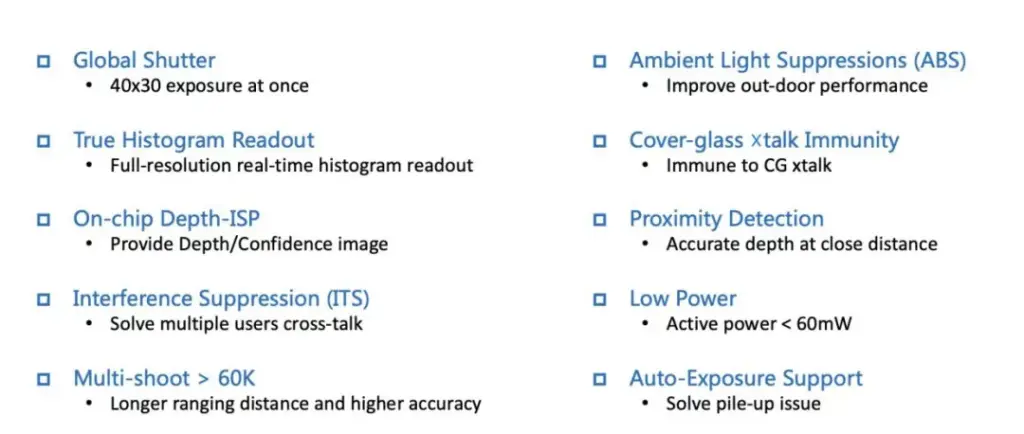
The VA6320 also incorporates Core Vision’s latest BSI SPAD sensor technology and deep isolation trench DTI process. These innovations deliver a detection efficiency seven times higher than conventional FSI technology, thereby providing superior detection performance in the near-infrared band and better PDE detection performance than the industry standard.
Further enhancements include a dynamic power management module, high-efficiency TDC, DSP computing module, and global shutter architecture, all integrated into the VA6320’s logic section. With these enhancements, the VA6320 can complete 1200-point depth detection simultaneously, boasting high frame rate, short exposure, and low power consumption.
To address the issue of photon accumulation caused by ambient light, Core Vision has optimized the VA6320’s TDC and logic modules for optical time-of-flight detection, yielding robust anti-sunlight performance. The VA6320 also integrates Core Vision’s Gen2 DSP deep signal processing module, which improves accuracy and resistance to environmental noise. With its MIPI interface, the VA6320 can output depth point cloud information with submillimeter precision at 60fps, along with the ability to output histograms at the original frame rate, offering greater scalability for back-end algorithms.