
At the recent imaginary (or is that virtual?) SID Display Week, two optimistic papers outlined advances in blue laser annealing (BLA) as a higher quality, less expensive, and much more scalable alternative to excimer laser annealing (ELA), which is today’s standard process for creating high performance backplanes.
In Distinguished Paper 3.1, authors from Jin Jang’s highly respected research group at the Advanced Display Research Center at Kyung Hee Univerisity described the development and characterization of a foldable LTPS TFT backplane using BLA. To understand BLA’s appeal lets first talk about ELA for a moment.
An excimer laser is a gas laser that, as used for displays, produces a line-shaped ultraviolet beam with a wavelength of 308 nm. The beam partially melts the surface of the amorphous-silicon-coated backplane. If this is done right — the processing window is tight — the silicon solidifies into polycrystalline silicon (polysilicon), which is a far more effective semiconductor than amorphous. Because making polysilicon this way does not heat the substrate very much, it is called low-temperature polysilicon (LTPS), and permits the use of relatively inexpensive glass substrates or polymer substrates.
ELA works but it has a number of drawbacks, one of which is that it does not scale well to substrate sizes larger than Gen 6 or 6.5. (one reason why Samsung was unable to make large RGB OLEDs for TVs – Editor) So, the OLED display in your smartphone uses ELA-fabricated LTPS and the OLED display in your TV set does not. And that brings us to annealing with blue lasers, which are diode — not gas — lasers.
Jang and his colleagues said,
“Due to high optical power density…of the active laser medium, diode lasers are packaged in a small form factor, and the laser beam can be coupled with standard optical fiber for convenient beam delivery, which can provide a tremendous advantage in scaling up BLA to large substrates such as G10.5.”
That would allow laser annealing to be used for volume production of LTPS backplanes for TV-sized OLEDs instead of the amorphous IGZO backplanes used today. When flexible polyimide OLEDs have been out-folded 30,000 times with a radius of 2.5mm, the threshold voltage of ELA TFTs shifted by more than 3 volts while the BLA threshold voltage shifts by less than 0.1 volt.
The team measured a high carrier mobility of 169 cm²/V·s and noted that the BLA process can be much less costly than a process using gas lasers, as well as producing a higher quality LTPS. (Excimer lasers are expensive and have a limited life, so have to be replaced regularly – Editor)
One Pixel at a Time
Paper 9.1, “Fabrication of Lateral Crystal Si on Cu Bottom-Gate Structure via Blue-Laser Diode Annealing (BLDA)” by Seiya Toriyama and his colleagues from V-Technology Company noted that the running cost of excimer lasers is expensive and that there can be a lack of uniformity in the resulting material that results in non-uniformity in the displayed image. He echoed Jang’s comments in saying that the cost of a BLDA system can be less than an ELA system, and that large single-crystal-lateral domains can be fabricated for improved carrier mobililty.
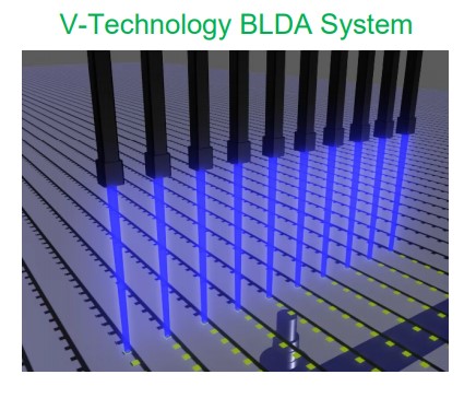 V-Technology’s Blue Laser Diode Annealing system delivers the laser light to the substrate via optical fires. The annealing of the silicon for each transistor is performed by the light from a single diode. (Graphic: V-Technology)
The authors thoroughly described their company’s technology of doing silicon crystallization on a copper electrode, and emphasized that their method crystallizes the silicon for each TFT with the light from a single blue-laser diode. The authors have successfully run the system at a scanning speed of 800mm/sec and a beam density of 491 kW/cm² without damage to the copper electrode material. Intended applications include miniLED backlights and TFT backplanes for OLED displays.
These are significant developments. Display Daily will continue to track them. (KW)
Ken Werner is Principal of Nutmeg Consultants, specializing in the display industry, manufacturing, technology, and applications, including mobile devices, automotive, and television. He consults for attorneys, investment analysts, and companies re-positioning themselves within the display industry or using displays in their products. He is the 2017 recipient of the Society for Information Display’s Lewis and Beatrice Winner Award. You can reach him at [email protected] or www.nutmegconsultants.com.