 Dr Neetu Chopra is from Kateeva which makes inkjet printing equipment for the thin film encapsulation (TFE) of OLEDs and is looking at how to do the patterning of OLEDs. It has recently boosted its facilities in California (Kateeva Doubles Its Factory Space for OLED Equipment) and now has 300 staff.
Kateeva sees the progression from rigid OLEDs to flexible now and to rollable in the future. The firm is supplying TFE equipment and claims a greater than 80% market share in inkjet TFE. It believes that the next generation technology evolution of inkjet is printing the OLED materials themselves.
For a half gen 6 OLED fab (that is one that uses substrates that have transistors added at G6, but where the display materials are added after the sheet is cut in half) a 1% loss in yield is $22 million and that’s more than the depreciation on cost of the inkjet equipment – so good equipment is very important. Delay in ramping up production is also an issue as one month’s delay in getting a fab up to good yield costs $165m – more than the cost of a printer. So the product has to be easy to buy, install and ramp.
The company has developed the software tools and inks for its machines and the process as well as metrology and process control. All of that technology is combined with an accurate printing table and an integrated printer solution.
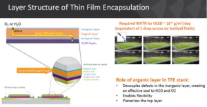
Chopra then showed the structure of the layers in TFE. There are organic and inorganic layers with the organic ones needed for flexibility. Discussed TFE – check slides – moisture diffusion can be tricky to control as the water vapour transfer rate has to be around 10-6 g/m²/day – that is the equivalent of a single drop across the area of six american football fields, per day.
At the moment, thermal evaporation is uesd that uses a lot of material and is difficult to get a good yield. Maintenance and cleaning costs are high. Ink jet material is much more efficient in material as well as achieving high surface planarisation.
The company is working on depositing inorganic materials and working on inks to try to achieve better spread. Films can be used for flexible substrates and making displays and Kateeva has tested bending for 100k cycles at a 3mm radius.
The company’s own R&D shows no roadblocks to using its existing printers to create truly flexible OLEDs and no real competition in TFE.
Moving to RGB layer fabrication, current technology uses white OLED with colour filter but it is inefficient. Vapour deposition is too difficult using shadow masks for large sized TV panels (which is why Samsung abandoned it, I believe – Man. Ed.) RGB beta testing is being done by Kateeva and some potential customers for field qualification. Inkjet is being further developed for deposition, but Chopra did not reveal any dates.
In the panel session at the end of the talks, Chopra said that the optimum launch time for inkjet deposition of OLED depends partly on the feature sizes needed. 80-145 ppi is the target range, which means attacking the 55″ market, although 200ppi is on the roadmap.