 Eric Virey is from Yole Développement and we have reported on his talks several times. He looked at MicroLED, asking if it was a viable alternative to OLED and LCD?
LED as a technology is already well understood and is now evolving. Virey sees a migration from LED to miniLED – which is not simply an interim technology. Some of the microLEDs which are under development are very small indeed and orders of magnitude smaller than traditional LEDs. Unfortunately, you can’t grow them on a large area substrate like an LCD or OLED – they are made using standard semiconductor techniques, but on 4″ to 8″ wafers. They then need singulating and mounting on the final surface.
LED has many advantages including very high brightness and that means only a small proportion of the surface of the display is needed for the LED itself – allowing lots of ideas for integrating sensors for example for fingerprint detection and ambient light measurement. It also allows a lot of black to give high contrast (like the Sony Cledis).
Lots of big technology companies have invested, from Apple onwards and there has been a big boost in the number of companies that are working on patents.
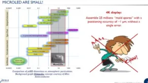
LEDs are widely available but Virey showed a very good slide comparing the size of microLEDs to spores and dust. Basically, building a microLED TV will be like “assembling 25 million mould spores with a positioning accuracy of 1?m without a single error”.
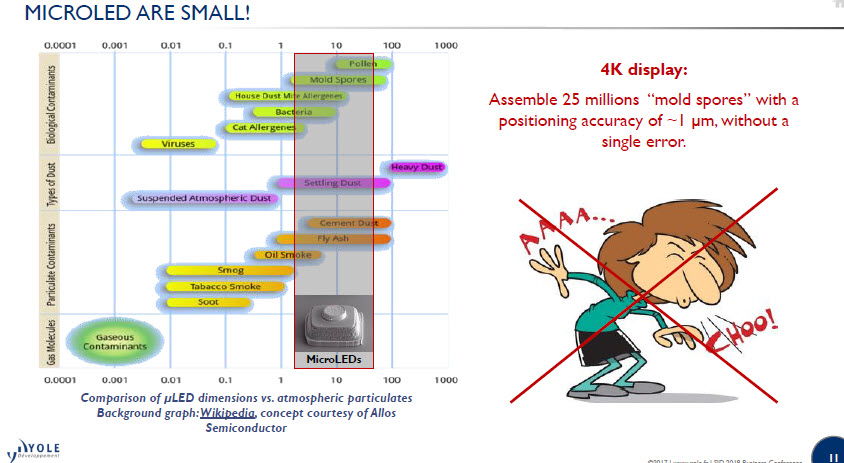 MicroLEDs are very small!
Placing the LEDs is a real challenge. An assembly rate of more than 100m chips per hour is likely to be needed and that will only make four sets per machine, per hour. Yield and defect management will be a real challenge, too. Testing and repair will be difficult at this kind of size. There have been some interesting ideas about how to do it, but there is likely to be an upstream yield strategy needed – you need to choose the good LEDs, with yield then place them, not repair after manufacture.
Yole said that 500 million LEDs could be made on a 6″ wafer – that’s a lot of testing.
You could try pixel redundancy although this doubles the cost of the dies and assembly. However, 99.99% placement accuracy may be realistic for good quality if you do this.
Virey talked about the Wall from Samsung – which is not a MicroLED and not, in his view a TV – the chips are simply too large. They are basically larger than 100 microns and probably around 125 x 225 (estimated), The total die cost for this kind of display would be $30,000 + $15,000 for assembly, so the list price could be 250K to $300K. There should be no panic buying on Black Friday! (Virey said he hadn’t heard pricing, but we have heard a cost of €150,000 for the commercial version, although we are not sure if that is distributor cost, or retail price).
If the size of the device can go down from 10?m to 5?m, the overall cost can go down. If you take every nth chip, it takes 30K cycles of a mass placement system to move the LCDs onto a TV. The largest area that could be used for a 6″ wafer would be around 170 blocks of 102 x 102mm – losing 20% of the wafer. Being clever could you get to 138 cycles with 20.7 x 18.7cm blocks. We’re not there yet, but we are in “the realm of the possible”.
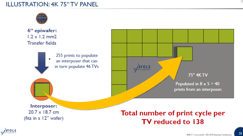 Assembly of MicroLED TVs needs to be clever to use all the LEDs on the wafer.
Companies are still making prototypes. The more advanced they are, the more challenges they find. There are no fundamental scientific challenges, but lots of engineering challenges. Yields are probably one of the biggest challenges.
Virey has said before, there is no established supply chain, so who takes the risk to build one? Clean rooms need to be much better than existing LED fabs, closer to CMOS fabs, but the makers who have those fabs have a lot of equipment they don’t need to make LEDs. The IP is spread out – Luxvue & Xcelprint are leading on patents, but no single company can have full freedom of operation.
Video walls are here with the Cledis from Sony. Smartwatches are relatively low hanging fruit as an application. AR & HUDs for that application is an opportunity while TV panel manuracture is probably doable for $200m to $300m plus capex for the fab in a couple of years, Virey believes. The smartphone market is difficult because of the low cost of current technologies.
Frontplane cost scales with the number of pixels, while the backplane scales with area. The displays could be driven by micro driver chips – which means that cost scales with number of pixels, not area – so a 110″ will not cost much more than 55″ to make, so very large TVs could be an early market.
On the other hand, OLED keeps improving, so TV is a moving target.
Analyst Comment
The other issue that was only briefly addressed by Virey is driving. LEDs are diodes and if you want to operate them efficiently, you really need to optimise the drive voltage and create grey scales using PWM. However, to get good low level grey scale, companies that make big LEDs drive them at more than 3,000Hz. That’s completely different from an OLED or LCD driving scheme, so existing substrate technologies could not be used, I don’t think, although I have heard that some kind of OLED-like approach may be possible. Perhaps companies will use current driving and just accept the power losses, but that would seem to reduce the advantages of going to microLEDs. I’d welcome feedback from anyone that has looked at this topic. (BR)