Avicena has been showcasing its LightBundle multi-Terabits per second (Tbps) chip-to-chip interconnect technology. This innovative MicroLED-based architecture is aiming to change perceptions and expectation in the performance of processors, memory, and sensors, addressing key bandwidth and proximity constraints while also delivering remarkable energy efficiency, according to the company.

The surge in demand for compute and memory performance, driven by applications like large language models (LLMs) such as ChatGPT, is primarily propelled by the rapid advancement of artificial intelligence (AI). These sophisticated AI models, including ChatGPT, exhibit an ever-growing hunger for computing power and fast memory access. Consequently, there is a pressing need for significantly higher-density, low-power interconnects between Graphics Processing Units (GPUs) and high-bandwidth memory (HBM) modules.
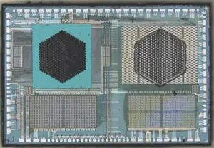
High-performance integrated circuits (ICs) today rely on SerDes-based electrical interfaces (serializer/deserializer) to achieve the necessary off-chip density. However, these electrical links suffer from power consumption and bandwidth density degradation as the link length increases. Traditional optical communication technologies, initially developed for networking applications, have proven unsuitable for interconnecting processors and processor-memory due to their low bandwidth density, high power consumption, and high cost. Conventional optical solutions often require external laser sources (ELS), adding complexity and cost to the setup. The LightBundle interconnect architecture leverages arrays of innovative Gallium Nitride (GaN) MicroLEDs, which can integrate onto high-performance CMOS ICs. Each MicroLED array is connected to a corresponding array of CMOS-compatible photodetectors (PDs) via a multi-core fiber cable.
Avicena is now advancing with their first ASIC in a 16-nanometer finFET process, boasting over 300 lanes and an impressive aggregate bandwidth exceeding 1 Terabit per second (Tbps) bi-directional at 4 Gbps per lane. The ASIC, compactly measuring less than 12 square millimeters, integrates the necessary circuitry for optical transmission and reception arrays, alongside a high-speed parallel electrical interface and various design for testability (DFT) and design for manufacturing (DFM) functions, such as bit error rate testing (BERT), loopbacks. All crucial ASIC functionalities have been validated, and efforts are ongoing to improve manufacturing yield for scalability.
LightBundle’s attributes, including low power consumption, high density, and minimal latency, make it a suitable fit for chiplet interfaces like UCIe, OpenHBI, and BoW. It also has the potential to improve system architectures currently limited by existing compute interconnects, such as PCIe/CXL and HBM/DDR/GDDR memory links.