Sixteen authors from institutions in Austria, Germany and Sweden recently reported on a technique to adjust the color of LED emissions using perovskites. This adjustment is done at the manufacturing stage, not in real-time as the LEDs are used. It does provide a way to make perovskite-based LEDs with wavelengths that are not native to perovskite materials. The full text of this paper, titled “Confining metal-halide perovskites in nanoporous thin films” is available online. A less technical explanation of the technique is also available at Phys.Org.
The advantage of the technique is the LEDs are not dependent on a GaN substrate. Eventually, if the research pans out, they will not require a rigid substrate of any material. Instead, the researchers believe that the resulting semiconductors can finally be printed on suitable materials, including flexible surfaces. Since solution-processed perovskites are a relatively well known technology, this technique should present no major problems in mass production and, in the future, may lead to the manufacture of pixelated RGB LEDs for use in flexible displays.
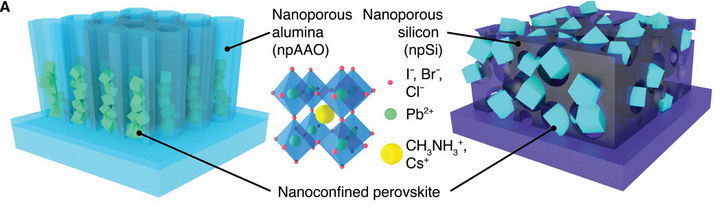 Various nanocrystaline perovskites in nanoporus alumina and silicon (credit: Stepan Demchyshyn et. al.)
To produce their color-tunable LEDs, the authors used nanoporous alumina (npAAO) or nanoporous silicon (npSi) scaffolds and grew metal-halide perovskite in the pores in the materials. The pores in both materials were made with an anodization process. For the npAAO nanoporus material, a thin film of aluminum 20nm – 1µm thick was evaporated on a glass substrate and converted to nanotubes about 8nm diameter by an anodization process. This process converted all the aluminum metal into alumina, leaving behind the nanotubes.
To make the npSi, boron-doped p-type silicon wafers with thickness of 0.5mm and <100> orientation were used. After preparation including polishing, the surface of the substrate was nanostructured by anodization. This is a well know, well controlled, silicon process step and nanoporus material with pore size from 2nm – 10nm can be made in a layer ten’s of microns thick. The authors state one of the next steps for their research is to replace the silicon wafer with thin-film silicon.
Note that even with the npSi, the perovskite is the light-emitting material in the LED, not the silicon. For example, with npSi and a cesium bromide perovskite, the researchers were able to produce LEDs with a narrow bandwidth, 17nm FWHM, on a transmissive conducting substrate. By varying the size of the pores, they could adjust the emission about 50nm, from the green that is native to cesium bromide to blue. The quantum confinement of the cesium bromide crystals in the nanopores is what shifts the wavelength. It does this by shifting the bandgap energy from the bulk perovskite material. The band-gap energy always increases in the nanocrystals, therefore the wavelength is always shifted toward shorter wavelengths, as shown in the figure.
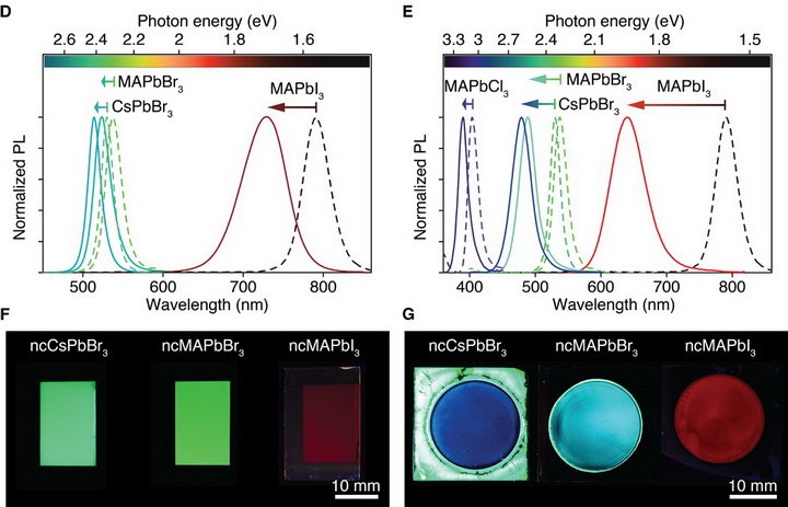 D&E: the wavelength shift and bandwidth achieved by the researchers with various perovskite materials. Dashed lines represent the properties of the bulk material. F&G: colors emitted by various materials. D&F are in alumina nanoporus thin film, E&G are in a nanoporus silicon. (credit: Stepan Demchyshyn et. al.)
An added benefit of the nanoporus alumina material is it encapsulates the perovskite crystals and protects them from the effects of oxygen and water vapor. On the other hand the authors report that it is easier to control the nanopore size in the silicon when the nanoporus layer is made.
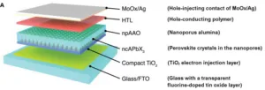
Structure of a LED based on nanoporus Alumina (Credit: Stepan Demchyshyn et. al. Additions in parentheses by M. Brennesholtz.)
The authors used the structure in the figure to make both red/nIR (731 nm) LEDs and cyan-green (518 nm) LEDs. The cyan-green LEDs used CsPbBr3 perovskite nanocrystal devices. These diodes turned on at ~2.5 V and give about 300 cd/m² operating at 5 V and a current density of about 420 mA/cm². This leads to a current efficiency of ~0.09 cd/A and an external quantum efficiency of ~0.03%. The authors state: “However, the demonstrated PLQY [photoluminescencent quantum yield] of up to 90% for our perovskite nanocrystals emitters suggests that higher efficiencies are achievable through further device optimization. This is expected to match the performance of current state-of-the-art 2D- and 3D-based perovskite LEDs while preserving the ease of color tuning.”
Analyst Comment
LEDs made in a research lab with a batch process on a rigid substrate are a long way from a printable RGB display. Nevertheless, this is a new approach to making LEDs and many (most?) of the materials used are compatible with printing or other roll-to-roll manufacturing techniques. As a bonus, any approach that provides a potential new path to green LEDs is welcome. While LEDs based on perovskite materials and nanoporus substrates are likely to be years away, they offer a way to address many wavelengths that are currently difficult to access using solution-processed perovskites. –Matthew Brennesholtz